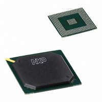
PNX1502E,557 NXP Semiconductors, PNX1502E,557 Datasheet - Page 152

PNX1502E,557
Manufacturer Part Number
PNX1502E,557
Description
IC MEDIA PROC 300MHZ 456-BGA
Manufacturer
NXP Semiconductors
Specifications of PNX1502E,557
Applications
Multimedia
Core Processor
TriMedia
Controller Series
Nexperia
Interface
I²C, 2-Wire Serial
Number Of I /o
61
Voltage - Supply
1.23 V ~ 1.37 V
Operating Temperature
0°C ~ 85°C
Mounting Type
Surface Mount
Package / Case
456-BGA
Lead Free Status / RoHS Status
Lead free / RoHS Compliant
Program Memory Type
-
Ram Size
-
Lead Free Status / Rohs Status
Not Compliant
Other names
935274744557
PNX1502E
PNX1502E
PNX1502E
PNX1502E
Available stocks
Company
Part Number
Manufacturer
Quantity
Price
Company:
Part Number:
PNX1502E,557
Manufacturer:
NXP Semiconductors
Quantity:
10 000
- Current page: 152 of 828
- Download datasheet (8Mb)
1. Introduction
2. Functional Description
The Clock module is the heart of the PNX15xx Series system. Its role is to provide
and control all the clocks of the system. The main characteristics of the Clock module
is to be low cost. It generates all the PNX15xx Series system clocks from one unique
source, a 27 MHz input crystal. The clock module features can be regrouped as
follows:
The Clock Module has three main internal interfaces:
A 27 MHz crystal clock provides the source clock for all PLLs in the CAB block and for
the low jitter PLL. The PLLs are programmable from the Clock module registers to
generate a range of possible frequencies. The DDS blocks are required to make
slight adjustments to each video and audio clock to track transmission sources.
Software controls this tracking by programming the relevant DDS block to adjust the
clock. These adjustments are made in steps of 0.4 Hz. The DDS clocks are derived
from the internal 1.728 GHz PLL (64 times the 27 MHz input crystal). The DDS jitter
is less than 0.58 ns. The video clock requirements may require a shorter term jitter so
an additional PLL is provided to smooth out the DDS jitter. This combines the two
video clock requirements, low jitter and high precision adjustment of the clock
frequency to meet color burst requirements but also track the audio signals.
The Clock Module consists of an MMIO-interface with programmable Clock and PLL
control registers, and a series of control logic for every clock generated. The clock
control logic will consist of:
•
•
•
•
•
•
Chapter 5: The Clock Module
PNX15xx Series Data Book – Volume 1 of 1
Rev. 3 — 17 March 2006
Use of Phase Locked Loop (PLL) circuits, Direct Digital Synthesizers (DDS) or
simple clock dividers to meet the frequency and jitter requirements of all
PNX15xx Series modules.
All the clocks are software programmable and support powerdown features.
Clock switching or clock frequency changes occur glitch free thank to dedicated
hardware.
an interface to a Custom Analog Block (CAB). The CAB module includes 2 PLLs,
several high speed clock dividers and 9 DDS blocks.
an interface to a dedicated low jitter PLL used for the DDR memory controller.
an MMIO interface to allow the programming of all configuration registers.
Product data sheet
Related parts for PNX1502E,557
Image
Part Number
Description
Manufacturer
Datasheet
Request
R
Part Number:
Description:
Digital Signal Processors & Controllers (DSP, DSC) MEDIA PROCESSOR PNX15XX/300MHZ
Manufacturer:
NXP Semiconductors

Part Number:
Description:
IC MEDIA PROC 300MHZ 456-BGA
Manufacturer:
NXP Semiconductors
Datasheet:
Part Number:
Description:
NXP Semiconductors designed the LPC2420/2460 microcontroller around a 16-bit/32-bitARM7TDMI-S CPU core with real-time debug interfaces that include both JTAG andembedded trace
Manufacturer:
NXP Semiconductors
Datasheet:

Part Number:
Description:
NXP Semiconductors designed the LPC2458 microcontroller around a 16-bit/32-bitARM7TDMI-S CPU core with real-time debug interfaces that include both JTAG andembedded trace
Manufacturer:
NXP Semiconductors
Datasheet:
Part Number:
Description:
NXP Semiconductors designed the LPC2468 microcontroller around a 16-bit/32-bitARM7TDMI-S CPU core with real-time debug interfaces that include both JTAG andembedded trace
Manufacturer:
NXP Semiconductors
Datasheet:
Part Number:
Description:
NXP Semiconductors designed the LPC2470 microcontroller, powered by theARM7TDMI-S core, to be a highly integrated microcontroller for a wide range ofapplications that require advanced communications and high quality graphic displays
Manufacturer:
NXP Semiconductors
Datasheet:
Part Number:
Description:
NXP Semiconductors designed the LPC2478 microcontroller, powered by theARM7TDMI-S core, to be a highly integrated microcontroller for a wide range ofapplications that require advanced communications and high quality graphic displays
Manufacturer:
NXP Semiconductors
Datasheet:
Part Number:
Description:
The Philips Semiconductors XA (eXtended Architecture) family of 16-bit single-chip microcontrollers is powerful enough to easily handle the requirements of high performance embedded applications, yet inexpensive enough to compete in the market for hi
Manufacturer:
NXP Semiconductors
Datasheet:
Part Number:
Description:
The XA-S3 device is a member of Philips Semiconductors? XA(eXtended Architecture) family of high performance 16-bitsingle-chip microcontrollers
Manufacturer:
NXP Semiconductors
Datasheet:

Part Number:
Description:
The NXP BlueStreak LH75401/LH75411 family consists of two low-cost 16/32-bit System-on-Chip (SoC) devices
Manufacturer:
NXP Semiconductors
Datasheet:

Part Number:
Description:
The NXP LPC3130/3131 combine an 180 MHz ARM926EJ-S CPU core, high-speed USB2
Manufacturer:
NXP Semiconductors
Datasheet:

Part Number:
Description:
The NXP LPC3141 combine a 270 MHz ARM926EJ-S CPU core, High-speed USB 2
Manufacturer:
NXP Semiconductors

Part Number:
Description:
The NXP LPC3143 combine a 270 MHz ARM926EJ-S CPU core, High-speed USB 2
Manufacturer:
NXP Semiconductors

Part Number:
Description:
The NXP LPC3152 combines an 180 MHz ARM926EJ-S CPU core, High-speed USB 2
Manufacturer:
NXP Semiconductors


