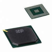
PNX1502E,557 NXP Semiconductors, PNX1502E,557 Datasheet - Page 198

PNX1502E,557
Manufacturer Part Number
PNX1502E,557
Description
IC MEDIA PROC 300MHZ 456-BGA
Manufacturer
NXP Semiconductors
Specifications of PNX1502E,557
Applications
Multimedia
Core Processor
TriMedia
Controller Series
Nexperia
Interface
I²C, 2-Wire Serial
Number Of I /o
61
Voltage - Supply
1.23 V ~ 1.37 V
Operating Temperature
0°C ~ 85°C
Mounting Type
Surface Mount
Package / Case
456-BGA
Lead Free Status / RoHS Status
Lead free / RoHS Compliant
Program Memory Type
-
Ram Size
-
Lead Free Status / Rohs Status
Not Compliant
Other names
935274744557
PNX1502E
PNX1502E
PNX1502E
PNX1502E
Available stocks
Company
Part Number
Manufacturer
Quantity
Price
Company:
Part Number:
PNX1502E,557
Manufacturer:
NXP Semiconductors
Quantity:
10 000
- Current page: 198 of 828
- Download datasheet (8Mb)
Philips Semiconductors
Volume 1 of 1
Table 11: CLOCK MODULE REGISTERS
PNX15XX_SER_3
Product data sheet
Bit
2:1
0
Offset 0x04,740C
31:4
3
2:1
0
Offset 0x04,7410
31:4
3
2:1
0
Offset 0x04,7414
31:9
8
7
6
Symbol
sel_clk_gpio_q6_12_ctl
en_clk_gpio_q6_12_ctl
Reserved
turn_off_ack
sel_clk_gpio_13_ctl
en_clk_gpio_13_ctl
Reserved
turn_off_ack
sel_clk_gpio_14_ctl
en_clk_gpio_14_ctl
Reserved
turn_off_ack
Invert_fgpo_clock
fgpo_output_select
CLK_GPIO_13_CTL
CLK_GPIO_14_CTL
CLK_FGPO_CTL
Acces
s
R/W
R/W
R/W
R
R/W
R/W
R/W
R
R/W
R/W
R/W
R
R/W
R/W
…Continued
Value
00
1
-
0
00
1
-
0
00
1
-
0
0
0
Rev. 3 — 17 March 2006
Description
00: clk_gpio_q6_12_ctl = 27 MHz xtal_clk
01: clk_gpio_q6_12_ctl = DDS6
10: clk_gpio_q6_12_ctl = 27 MHz xtal_clk
11: clk_gpio_q6_12_ctl = LAN_TXD[3]
1: enable clk_gpio_q6_12_ctl
To ensure software backward compatibility unused or reserved bits
must be written as zeros and ignored upon read.
0 - Indicates if the enabled clock is running
1 - Indicates that the clock is being blocked during a frequency
change to avoid glitches
00: clk_gpio_13_ctl = 27 MHz xtal_clk
01: clk_gpio_13_ctl = DDS5
10: clk_gpio_13_ctl = UNDEF
11: clk_gpio_13_ctl = LAN_RXD[0]
1: enable clk_gpio_13_ctl
To ensure software backward compatibility unused or reserved bits
must be written as zeros and ignored upon read.
0 - Indicates if the enabled clock is running
1 - Indicates that the clock is being blocked during a frequency
change to avoid glitches
00: clk_gpio_14_ctl = 27 MHz xtal_clk
01: clk_gpio_14_ctl = DDS2
10: clk_gpio_14_ctl = UNDEF
11: clk_gpio_14_ctl = LAN_RXD[1]
1: enable clk_gpio_14_ctl
To ensure software backward compatibility unused or reserved bits
must be written as zeros and ignored upon read.
0 - Indicates if the enabled clock is running
1 - Indicates that the clock is being blocked during a frequency
change to avoid glitches
Invert FGPO clock
0 : do not invert the clock
1: invert the clock only to the fgpo block and not to the pad.
FGPO output select
0: Seperate output mode, The clock to the fgpo and to the pad
share the same source, but have seperate paths.
1: Feedback output mode, The clock is driven to the pad then is
feedback to the clock block. It then goes through gating logic to the
fgpo block.
Chapter 5: The Clock Module
© Koninklijke Philips Electronics N.V. 2006. All rights reserved.
PNX15xx Series
5-47
Related parts for PNX1502E,557
Image
Part Number
Description
Manufacturer
Datasheet
Request
R
Part Number:
Description:
Digital Signal Processors & Controllers (DSP, DSC) MEDIA PROCESSOR PNX15XX/300MHZ
Manufacturer:
NXP Semiconductors

Part Number:
Description:
IC MEDIA PROC 300MHZ 456-BGA
Manufacturer:
NXP Semiconductors
Datasheet:
Part Number:
Description:
NXP Semiconductors designed the LPC2420/2460 microcontroller around a 16-bit/32-bitARM7TDMI-S CPU core with real-time debug interfaces that include both JTAG andembedded trace
Manufacturer:
NXP Semiconductors
Datasheet:

Part Number:
Description:
NXP Semiconductors designed the LPC2458 microcontroller around a 16-bit/32-bitARM7TDMI-S CPU core with real-time debug interfaces that include both JTAG andembedded trace
Manufacturer:
NXP Semiconductors
Datasheet:
Part Number:
Description:
NXP Semiconductors designed the LPC2468 microcontroller around a 16-bit/32-bitARM7TDMI-S CPU core with real-time debug interfaces that include both JTAG andembedded trace
Manufacturer:
NXP Semiconductors
Datasheet:
Part Number:
Description:
NXP Semiconductors designed the LPC2470 microcontroller, powered by theARM7TDMI-S core, to be a highly integrated microcontroller for a wide range ofapplications that require advanced communications and high quality graphic displays
Manufacturer:
NXP Semiconductors
Datasheet:
Part Number:
Description:
NXP Semiconductors designed the LPC2478 microcontroller, powered by theARM7TDMI-S core, to be a highly integrated microcontroller for a wide range ofapplications that require advanced communications and high quality graphic displays
Manufacturer:
NXP Semiconductors
Datasheet:
Part Number:
Description:
The Philips Semiconductors XA (eXtended Architecture) family of 16-bit single-chip microcontrollers is powerful enough to easily handle the requirements of high performance embedded applications, yet inexpensive enough to compete in the market for hi
Manufacturer:
NXP Semiconductors
Datasheet:
Part Number:
Description:
The XA-S3 device is a member of Philips Semiconductors? XA(eXtended Architecture) family of high performance 16-bitsingle-chip microcontrollers
Manufacturer:
NXP Semiconductors
Datasheet:

Part Number:
Description:
The NXP BlueStreak LH75401/LH75411 family consists of two low-cost 16/32-bit System-on-Chip (SoC) devices
Manufacturer:
NXP Semiconductors
Datasheet:

Part Number:
Description:
The NXP LPC3130/3131 combine an 180 MHz ARM926EJ-S CPU core, high-speed USB2
Manufacturer:
NXP Semiconductors
Datasheet:

Part Number:
Description:
The NXP LPC3141 combine a 270 MHz ARM926EJ-S CPU core, High-speed USB 2
Manufacturer:
NXP Semiconductors

Part Number:
Description:
The NXP LPC3143 combine a 270 MHz ARM926EJ-S CPU core, High-speed USB 2
Manufacturer:
NXP Semiconductors

Part Number:
Description:
The NXP LPC3152 combines an 180 MHz ARM926EJ-S CPU core, High-speed USB 2
Manufacturer:
NXP Semiconductors


