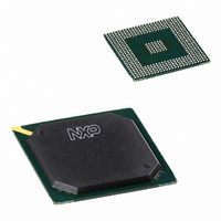
PNX1502E,557 NXP Semiconductors, PNX1502E,557 Datasheet - Page 79

PNX1502E,557
Manufacturer Part Number
PNX1502E,557
Description
IC MEDIA PROC 300MHZ 456-BGA
Manufacturer
NXP Semiconductors
Specifications of PNX1502E,557
Applications
Multimedia
Core Processor
TriMedia
Controller Series
Nexperia
Interface
I²C, 2-Wire Serial
Number Of I /o
61
Voltage - Supply
1.23 V ~ 1.37 V
Operating Temperature
0°C ~ 85°C
Mounting Type
Surface Mount
Package / Case
456-BGA
Lead Free Status / RoHS Status
Lead free / RoHS Compliant
Program Memory Type
-
Ram Size
-
Lead Free Status / Rohs Status
Not Compliant
Other names
935274744557
PNX1502E
PNX1502E
PNX1502E
PNX1502E
Available stocks
Company
Part Number
Manufacturer
Quantity
Price
Company:
Part Number:
PNX1502E,557
Manufacturer:
NXP Semiconductors
Quantity:
10 000
- Current page: 79 of 828
- Download datasheet (8Mb)
Philips Semiconductors
Volume 1 of 1
PNX15XX_SER_3
Product data sheet
10.3.1 Do DDR Devices Require Termination?
10.3.2 What if I really want to use termination for the PNX1500?
Table 44: DDR Recommended Trance Length
DDR devices that are DDR400{A,B,C} JEDEC compliant, revision JESD79C, have
tDQSS defined as 0.72*tCK (min) and 1.25*tCK (max). Faster DDR devices have a
more stringent requirement of 0.8*tCK and 1.2*tCK or even 0.85*tCK and 1.15*tCK.
The PNX1500 can support these fast DDR devices as long as
followed. In case of using DDR400 only DDR devices, MM_CK/MM_CK# may have a
minimum value of 4 cm, the remaining signals should still follow as close as possible
the
The ball assignment implies that the two outside rows of balls are routed on a
different board layer than the next two rows of balls. This is recommended to reduce
the skew. The DQS lines are the exception since they are located on the outside row
for better package signal integrity.
A 10-22
placed as close as possible to the PNX1500 clock output pins. In addition a 100
shunting both memory clocks, i.e. MM_CLK and MM_CLK#, will reduce the swing of
the signals and improve signal integrity. The 100
devices.
No other termination is required at board level to achieve maximum speed if these
rules are strictly followed.
Above DDR333, i.e. MM_CLK of 166 MHz, the 183 or 200 MHz operating speeds (i.e.
DDR400) are only available for a maximum of 2 loads.
VREF, a.k.a. AVREF, can be generated by using a simple voltage resistor divider. 100
one local VREF for PNX1500 and one local VREF for the DDRs is slightly better.
Most DDR devices are meant to drive very long and highly loaded track lines. Their
drivers are usually very strong and could use a 22
and dqs lines on the DDR device’s end.
It is possible to parallel terminate each line to a termination voltage with a 50
resistor to avoid over-undershoots and therefore potential too high EMC/EMI noise.
The resistor should be placed as close as possible to the intersection of the leg of ‘T’
Signal
MM_CK, MM_CK#
MM_AD[12:0], MM_BA[1:0]
MM_RAS/CAS/WE/CKE
MM_CS[1:0]
MM_DQS[3:0]
MM_DATA[31:0]
MM_DQM[3:0]
•
to 150
Table
Recommended Trace lengths for operating frequency of up to DDR400 are
shown in
44.
series resistor is recommended on the two clock lines. They need to be
1% resistors are recommended. VREF should be on a wide trace. Having
Table
Rev. 3 — 17 March 2006
44.
Maximum (cm)
4
7
3
3
Chapter 1: Integrated Circuit Data
can be placed after the DDR
series resistors on the data/dqm
© Koninklijke Philips Electronics N.V. 2006. All rights reserved.
Minimum (cm)
4
2
3
1
PNX15xx Series
Table 44
is strictly
1-52
Related parts for PNX1502E,557
Image
Part Number
Description
Manufacturer
Datasheet
Request
R
Part Number:
Description:
Digital Signal Processors & Controllers (DSP, DSC) MEDIA PROCESSOR PNX15XX/300MHZ
Manufacturer:
NXP Semiconductors

Part Number:
Description:
IC MEDIA PROC 300MHZ 456-BGA
Manufacturer:
NXP Semiconductors
Datasheet:
Part Number:
Description:
NXP Semiconductors designed the LPC2420/2460 microcontroller around a 16-bit/32-bitARM7TDMI-S CPU core with real-time debug interfaces that include both JTAG andembedded trace
Manufacturer:
NXP Semiconductors
Datasheet:

Part Number:
Description:
NXP Semiconductors designed the LPC2458 microcontroller around a 16-bit/32-bitARM7TDMI-S CPU core with real-time debug interfaces that include both JTAG andembedded trace
Manufacturer:
NXP Semiconductors
Datasheet:
Part Number:
Description:
NXP Semiconductors designed the LPC2468 microcontroller around a 16-bit/32-bitARM7TDMI-S CPU core with real-time debug interfaces that include both JTAG andembedded trace
Manufacturer:
NXP Semiconductors
Datasheet:
Part Number:
Description:
NXP Semiconductors designed the LPC2470 microcontroller, powered by theARM7TDMI-S core, to be a highly integrated microcontroller for a wide range ofapplications that require advanced communications and high quality graphic displays
Manufacturer:
NXP Semiconductors
Datasheet:
Part Number:
Description:
NXP Semiconductors designed the LPC2478 microcontroller, powered by theARM7TDMI-S core, to be a highly integrated microcontroller for a wide range ofapplications that require advanced communications and high quality graphic displays
Manufacturer:
NXP Semiconductors
Datasheet:
Part Number:
Description:
The Philips Semiconductors XA (eXtended Architecture) family of 16-bit single-chip microcontrollers is powerful enough to easily handle the requirements of high performance embedded applications, yet inexpensive enough to compete in the market for hi
Manufacturer:
NXP Semiconductors
Datasheet:
Part Number:
Description:
The XA-S3 device is a member of Philips Semiconductors? XA(eXtended Architecture) family of high performance 16-bitsingle-chip microcontrollers
Manufacturer:
NXP Semiconductors
Datasheet:

Part Number:
Description:
The NXP BlueStreak LH75401/LH75411 family consists of two low-cost 16/32-bit System-on-Chip (SoC) devices
Manufacturer:
NXP Semiconductors
Datasheet:

Part Number:
Description:
The NXP LPC3130/3131 combine an 180 MHz ARM926EJ-S CPU core, high-speed USB2
Manufacturer:
NXP Semiconductors
Datasheet:

Part Number:
Description:
The NXP LPC3141 combine a 270 MHz ARM926EJ-S CPU core, High-speed USB 2
Manufacturer:
NXP Semiconductors

Part Number:
Description:
The NXP LPC3143 combine a 270 MHz ARM926EJ-S CPU core, High-speed USB 2
Manufacturer:
NXP Semiconductors

Part Number:
Description:
The NXP LPC3152 combines an 180 MHz ARM926EJ-S CPU core, High-speed USB 2
Manufacturer:
NXP Semiconductors


