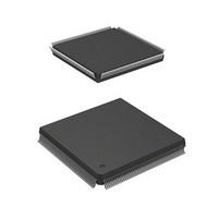
HD6417750RF240DV Renesas Electronics America, HD6417750RF240DV Datasheet - Page 208

HD6417750RF240DV
Manufacturer Part Number
HD6417750RF240DV
Description
MPU 3V 16K I-TEMP,PB-FREE 208-QF
Manufacturer
Renesas Electronics America
Series
SuperH® SH7750r
Datasheet
1.D6417750RBP240DV.pdf
(1164 pages)
Specifications of HD6417750RF240DV
Core Processor
SH-4
Core Size
32-Bit
Speed
240MHz
Connectivity
EBI/EMI, FIFO, SCI, SmartCard
Peripherals
DMA, POR, WDT
Number Of I /o
28
Program Memory Type
ROMless
Ram Size
48K x 8
Voltage - Supply (vcc/vdd)
1.4 V ~ 1.6 V
Oscillator Type
External
Operating Temperature
-40°C ~ 85°C
Package / Case
208-QFP
Lead Free Status / RoHS Status
Lead free / RoHS Compliant
Eeprom Size
-
Program Memory Size
-
Data Converters
-
Available stocks
Company
Part Number
Manufacturer
Quantity
Price
Company:
Part Number:
HD6417750RF240DV
Manufacturer:
HITACHI
Quantity:
7 287
- Current page: 208 of 1164
- Download datasheet (7Mb)
Section 4 Caches
3e. Cache miss (with copy-back/write-back)
4.3.4
In order to give priority to data reads to the cache and improve performance, this LSI has a write-
back buffer which holds the relevant cache entry when it becomes necessary to purge a dirty cache
entry into external memory as the result of a cache miss. The write-back buffer contains one cache
line of data and the physical address of the purge destination.
4.3.5
This LSI has a 64-bit buffer for holding write data when writing data in write-through mode or
writing to a non-cacheable area. This allows the CPU to proceed to the next operation as soon as
the write to the write-through buffer is completed, without waiting for completion of the write to
external memory.
Rev.7.00 Oct. 10, 2008 Page 122 of 1074
REJ09B0366-0700
The tag and data field of the cache line indexed by effective address bits [13:5] are first saved
in the write-back buffer, and then a data write in accordance with the access size
(quadword/longword/word/byte) is performed for the data indexed by bits [4:0] of the effective
address of the data field of the cache line indexed by effective address bits [13:5]. Then, data is
read into the cache line from the external memory space corresponding to the effective
address. Data reading is performed, using the wraparound method, in order from the longword
data corresponding to the effective address, and one cache line of data is read excluding the
written data. During this time, the CPU can execute the next processing. When reading of one
line of data is completed, the tag corresponding to the effective address is recorded in the
cache, and 1 is written to the V bit and U bit. The data in the write-back buffer is then written
back to external memory.
Physical address bits [28:5]
Write-Back Buffer
Write-Through Buffer
Figure 4.5 Configuration of Write-Through Buffer
Figure 4.4 Configuration of Write-Back Buffer
Physical address bits [28:0]
LW0
LW1
LW2
LW3
LW0
LW4
LW1
LW5
LW6
LW7
Related parts for HD6417750RF240DV
Image
Part Number
Description
Manufacturer
Datasheet
Request
R

Part Number:
Description:
KIT STARTER FOR M16C/29
Manufacturer:
Renesas Electronics America
Datasheet:

Part Number:
Description:
KIT STARTER FOR R8C/2D
Manufacturer:
Renesas Electronics America
Datasheet:

Part Number:
Description:
R0K33062P STARTER KIT
Manufacturer:
Renesas Electronics America
Datasheet:

Part Number:
Description:
KIT STARTER FOR R8C/23 E8A
Manufacturer:
Renesas Electronics America
Datasheet:

Part Number:
Description:
KIT STARTER FOR R8C/25
Manufacturer:
Renesas Electronics America
Datasheet:

Part Number:
Description:
KIT STARTER H8S2456 SHARPE DSPLY
Manufacturer:
Renesas Electronics America
Datasheet:

Part Number:
Description:
KIT STARTER FOR R8C38C
Manufacturer:
Renesas Electronics America
Datasheet:

Part Number:
Description:
KIT STARTER FOR R8C35C
Manufacturer:
Renesas Electronics America
Datasheet:

Part Number:
Description:
KIT STARTER FOR R8CL3AC+LCD APPS
Manufacturer:
Renesas Electronics America
Datasheet:

Part Number:
Description:
KIT STARTER FOR RX610
Manufacturer:
Renesas Electronics America
Datasheet:

Part Number:
Description:
KIT STARTER FOR R32C/118
Manufacturer:
Renesas Electronics America
Datasheet:

Part Number:
Description:
KIT DEV RSK-R8C/26-29
Manufacturer:
Renesas Electronics America
Datasheet:

Part Number:
Description:
KIT STARTER FOR SH7124
Manufacturer:
Renesas Electronics America
Datasheet:

Part Number:
Description:
KIT STARTER FOR H8SX/1622
Manufacturer:
Renesas Electronics America
Datasheet:

Part Number:
Description:
KIT DEV FOR SH7203
Manufacturer:
Renesas Electronics America
Datasheet:


