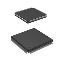
HD6417750RF240DV Renesas Electronics America, HD6417750RF240DV Datasheet - Page 549

HD6417750RF240DV
Manufacturer Part Number
HD6417750RF240DV
Description
MPU 3V 16K I-TEMP,PB-FREE 208-QF
Manufacturer
Renesas Electronics America
Series
SuperH® SH7750r
Datasheet
1.D6417750RBP240DV.pdf
(1164 pages)
Specifications of HD6417750RF240DV
Core Processor
SH-4
Core Size
32-Bit
Speed
240MHz
Connectivity
EBI/EMI, FIFO, SCI, SmartCard
Peripherals
DMA, POR, WDT
Number Of I /o
28
Program Memory Type
ROMless
Ram Size
48K x 8
Voltage - Supply (vcc/vdd)
1.4 V ~ 1.6 V
Oscillator Type
External
Operating Temperature
-40°C ~ 85°C
Package / Case
208-QFP
Lead Free Status / RoHS Status
Lead free / RoHS Compliant
Eeprom Size
-
Program Memory Size
-
Data Converters
-
Available stocks
Company
Part Number
Manufacturer
Quantity
Price
Company:
Part Number:
HD6417750RF240DV
Manufacturer:
HITACHI
Quantity:
7 287
- Current page: 549 of 1164
- Download datasheet (7Mb)
• Self-Refresh
• Relationship between Refresh Requests and Bus Cycle Requests
The self-refreshing supported by this LSI is shown in figure 13.25.
After the self-refresh is cleared, the refresh controller immediately generates a refresh request.
The RAS precharge time immediately after the end of the self-refreshing can be set by bits
TRC2–TRC0 in MCR.
CAS-before-RAS refreshing is performed in normal operation, in sleep mode, and in the case
of a manual reset.
Self-refreshing is performed in normal operation, in sleep mode, in standby mode, and in the
case of a manual reset.
When the bus has been released in response to a bus arbitration request, or when a transition is
made to standby mode, signals generally become high-impedance, but whether the RAS and
CAS signals become high-impedance or continue to be output can be controlled by the
HIZCNT bit in BCR1. This enables the DRAM to be kept in the self-refreshing state.
As the DRAM CAS signal is multiplexed with WEn for normal memory (SRAM, etc.), access
to memory that uses the WEn signals must be disabled during self-refreshing.
If a refresh request is generated during execution of a bus cycle, execution of the refresh is
deferred until the bus cycle is completed. Refresh operations are deferred during multiple bus
cycles generated because the data bus width is smaller than the access size (for example, when
performing longword access to 8-bit bus width memory) and during a 32-byte transfer such as
a cache fill or write-back, and also between read and write cycles during execution of a TAS
instruction, and between read and write cycles when DMAC dual address transfer is executed.
If a refresh request occurs when the bus has been released by the bus arbiter, refresh execution
is deferred until the bus is acquired. If a match between RTCNT and RTCOR occurs while a
refresh is waiting to be executed, so that a new refresh request is generated, the previous
refresh request is eliminated. In order for refreshing to be performed normally, care must be
taken to ensure that no bus cycle or bus mastership occurs that is longer than the refresh
interval. When a refresh request is generated, the BACK pin is negated (driven high).
Therefore, normal refreshing can be performed by having the BACK pin monitored by a bus
master other than this LSI requesting the bus, or the bus arbiter, and returning the bus to this
LSI.
Rev.7.00 Oct. 10, 2008 Page 463 of 1074
Section 13 Bus State Controller (BSC)
REJ09B0366-0700
Related parts for HD6417750RF240DV
Image
Part Number
Description
Manufacturer
Datasheet
Request
R

Part Number:
Description:
KIT STARTER FOR M16C/29
Manufacturer:
Renesas Electronics America
Datasheet:

Part Number:
Description:
KIT STARTER FOR R8C/2D
Manufacturer:
Renesas Electronics America
Datasheet:

Part Number:
Description:
R0K33062P STARTER KIT
Manufacturer:
Renesas Electronics America
Datasheet:

Part Number:
Description:
KIT STARTER FOR R8C/23 E8A
Manufacturer:
Renesas Electronics America
Datasheet:

Part Number:
Description:
KIT STARTER FOR R8C/25
Manufacturer:
Renesas Electronics America
Datasheet:

Part Number:
Description:
KIT STARTER H8S2456 SHARPE DSPLY
Manufacturer:
Renesas Electronics America
Datasheet:

Part Number:
Description:
KIT STARTER FOR R8C38C
Manufacturer:
Renesas Electronics America
Datasheet:

Part Number:
Description:
KIT STARTER FOR R8C35C
Manufacturer:
Renesas Electronics America
Datasheet:

Part Number:
Description:
KIT STARTER FOR R8CL3AC+LCD APPS
Manufacturer:
Renesas Electronics America
Datasheet:

Part Number:
Description:
KIT STARTER FOR RX610
Manufacturer:
Renesas Electronics America
Datasheet:

Part Number:
Description:
KIT STARTER FOR R32C/118
Manufacturer:
Renesas Electronics America
Datasheet:

Part Number:
Description:
KIT DEV RSK-R8C/26-29
Manufacturer:
Renesas Electronics America
Datasheet:

Part Number:
Description:
KIT STARTER FOR SH7124
Manufacturer:
Renesas Electronics America
Datasheet:

Part Number:
Description:
KIT STARTER FOR H8SX/1622
Manufacturer:
Renesas Electronics America
Datasheet:

Part Number:
Description:
KIT DEV FOR SH7203
Manufacturer:
Renesas Electronics America
Datasheet:


