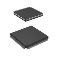
HD6417750RF240DV Renesas Electronics America, HD6417750RF240DV Datasheet - Page 627

HD6417750RF240DV
Manufacturer Part Number
HD6417750RF240DV
Description
MPU 3V 16K I-TEMP,PB-FREE 208-QF
Manufacturer
Renesas Electronics America
Series
SuperH® SH7750r
Datasheet
1.D6417750RBP240DV.pdf
(1164 pages)
Specifications of HD6417750RF240DV
Core Processor
SH-4
Core Size
32-Bit
Speed
240MHz
Connectivity
EBI/EMI, FIFO, SCI, SmartCard
Peripherals
DMA, POR, WDT
Number Of I /o
28
Program Memory Type
ROMless
Ram Size
48K x 8
Voltage - Supply (vcc/vdd)
1.4 V ~ 1.6 V
Oscillator Type
External
Operating Temperature
-40°C ~ 85°C
Package / Case
208-QFP
Lead Free Status / RoHS Status
Lead free / RoHS Compliant
Eeprom Size
-
Program Memory Size
-
Data Converters
-
Available stocks
Company
Part Number
Manufacturer
Quantity
Price
Company:
Part Number:
HD6417750RF240DV
Manufacturer:
HITACHI
Quantity:
7 287
- Current page: 627 of 1164
- Download datasheet (7Mb)
Section 13 Bus State Controller (BSC)
13.3.14 Partial-Sharing Master Mode
In partial-sharing master mode, area 2 only is shared with other devices, and other areas can be
accessed at all times. Partial-sharing master mode can be set by setting master mode with the
external mode pins, and setting the PSHR bit to 1 in BCR1 in the initialization procedure in a
power-on reset. Do not access area 2 until these settings have been performed. In a manual reset
the bus state controller setting register values are retained, and so need not be set again.
Partial-sharing master mode is designed for use in conjunction with a master mode chip. The
partial-sharing master can access a device on the master side via area 2, but the master cannot
access a device on the partial-sharing master side.
An address and control signal buffer and a data buffer must be located between the partial-sharing
master and the master, and controlled by a buffer control circuit.
The partial-sharing master mode processor uses the following procedure to access area 2. It asserts
the BSREQ signal on the rising edge of the clock, and issues a bus request to the master. It
samples BSACK on each rising edge of the clock, and on receiving BSACK assertion, starts the
access cycle on the next rising edge of the clock. At the end of the access, it negates BSREQ on
the rising edge of the clock. Buffer control in an access to an area 2 device by the partial-sharing
master is carried out by referencing the CS2 signal or BSREQ and BSACK signals on the partial-
sharing master side. Permission to use the bus is reported by the BSACK line connected to the
partial-sharing master, but the master may also negate the BSACK signal even while the bus is
being used, if it needs the bus urgently in order to service a refresh, for example. Consequently,
the partial-sharing master has to monitor the BSREQ signal to see whether it can continue to use
the bus after detecting BSACK assertion. In the case of the address buffer, after the address buffer
is turned on when BSACK assertion is detected, the buffer is kept on until BSREQ is negated, at
which point it is turned off. If the turning-off of the buffer used is late, resulting in a collision with
the start of an access cycle on the master side, the BSREQ signal output from the partial-sharing
master must be routed through a delay circuit as part of the buffer control circuit, and input to the
master BREQ signal.
In order for a partial-sharing master mode processor to begin area 2 access, the BSACK signal
must be asserted for at least two cycles.
When the bus is released after area 2 has been accessed in partial-sharing master mode, if area 2 is
synchronous DRAM, there is a wait of the period required for auto-precharge before bus release is
performed.
In partial-sharing master mode, refreshing is not performed for area 2 (refresh requests are
ignored).
Rev.7.00 Oct. 10, 2008 Page 541 of 1074
REJ09B0366-0700
Related parts for HD6417750RF240DV
Image
Part Number
Description
Manufacturer
Datasheet
Request
R

Part Number:
Description:
KIT STARTER FOR M16C/29
Manufacturer:
Renesas Electronics America
Datasheet:

Part Number:
Description:
KIT STARTER FOR R8C/2D
Manufacturer:
Renesas Electronics America
Datasheet:

Part Number:
Description:
R0K33062P STARTER KIT
Manufacturer:
Renesas Electronics America
Datasheet:

Part Number:
Description:
KIT STARTER FOR R8C/23 E8A
Manufacturer:
Renesas Electronics America
Datasheet:

Part Number:
Description:
KIT STARTER FOR R8C/25
Manufacturer:
Renesas Electronics America
Datasheet:

Part Number:
Description:
KIT STARTER H8S2456 SHARPE DSPLY
Manufacturer:
Renesas Electronics America
Datasheet:

Part Number:
Description:
KIT STARTER FOR R8C38C
Manufacturer:
Renesas Electronics America
Datasheet:

Part Number:
Description:
KIT STARTER FOR R8C35C
Manufacturer:
Renesas Electronics America
Datasheet:

Part Number:
Description:
KIT STARTER FOR R8CL3AC+LCD APPS
Manufacturer:
Renesas Electronics America
Datasheet:

Part Number:
Description:
KIT STARTER FOR RX610
Manufacturer:
Renesas Electronics America
Datasheet:

Part Number:
Description:
KIT STARTER FOR R32C/118
Manufacturer:
Renesas Electronics America
Datasheet:

Part Number:
Description:
KIT DEV RSK-R8C/26-29
Manufacturer:
Renesas Electronics America
Datasheet:

Part Number:
Description:
KIT STARTER FOR SH7124
Manufacturer:
Renesas Electronics America
Datasheet:

Part Number:
Description:
KIT STARTER FOR H8SX/1622
Manufacturer:
Renesas Electronics America
Datasheet:

Part Number:
Description:
KIT DEV FOR SH7203
Manufacturer:
Renesas Electronics America
Datasheet:


