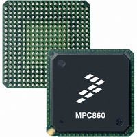
MC68360VR25VL Freescale Semiconductor, MC68360VR25VL Datasheet - Page 684

MC68360VR25VL
Manufacturer Part Number
MC68360VR25VL
Description
IC MPU QUICC 25MHZ 357-PBGA
Manufacturer
Freescale Semiconductor
Datasheets
1.MC68EN360VR25L.pdf
(14 pages)
2.MC68EN360VR25L.pdf
(2 pages)
3.MC68360AI25L.pdf
(962 pages)
Specifications of MC68360VR25VL
Processor Type
M683xx 32-Bit
Speed
25MHz
Voltage
3.3V
Mounting Type
Surface Mount
Package / Case
357-PBGA
Family Name
M68000
Device Core
ColdFire
Device Core Size
32b
Frequency (max)
25MHz
Instruction Set Architecture
RISC
Operating Supply Voltage (max)
3.3V
Operating Supply Voltage (min)
2.7V
Operating Temp Range
0C to 70C
Operating Temperature Classification
Commercial
Mounting
Surface Mount
Pin Count
357
Package Type
BGA
Lead Free Status / RoHS Status
Lead free / RoHS Compliant
Features
-
Lead Free Status / Rohs Status
Compliant
Available stocks
Company
Part Number
Manufacturer
Quantity
Price
Company:
Part Number:
MC68360VR25VL
Manufacturer:
Exar
Quantity:
160
Company:
Part Number:
MC68360VR25VL
Manufacturer:
Freescale Semiconductor
Quantity:
10 000
Company:
Part Number:
MC68360VR25VLR2
Manufacturer:
Freescale Semiconductor
Quantity:
10 000
- Current page: 684 of 962
- Download datasheet (4Mb)
Parallel I/O Ports
For each DDx bit, the definition is as follows:
7.14.5 Port A Examples
The following paragraphs discuss various ways some of the port A pins can be configured.
Figure 7-97 and Figure 7-98 show block diagrams of the PA0 and PA1 pins.
PA0 can be configured as a general-purpose I/O pin, but not an open-drain pin. It may also
be the RXD1 pin for SCC1 in the NMSI mode. If PA0 is configured as a general-purpose I/
O pin, then the RXD1 input is internally grounded. If SCC1 is connected to a TDM or is not
used, then PA0 may be used as general-purpose I/O.
PA1 can be configured as a general-purpose I/O pin, either open-drain or not. It may also
be the TXD1 pin for SCC1 in the NMSI mode. If TXD1 is configured as an output on PA1
and the OD1 bit is set in PAODR, then TXD1 will be output from SCC1 as an open-drain
output. If PA1 is configured as a general-purpose I/O pin, then the TXD1 output is not con-
nected externally. If SCC1 is connected to a TDM or is not used, then PA1 may be used as
a general-purpose I/O.
7-360
0 = General-purpose I/O. The peripheral functions of the pin are not used.
1 = Dedicated peripheral function. The pin is used by the internal module. The
SCC1
TO
PADAT
BIT 0
TO
on-chip peripheral function to which it is dedicated may be determined by other bits
such as those is the PADIR.
PORT C11–PORT C0
RXD1
RISC TIMER TABLE
SDMA BUS ERROR
SOURCES
INTERMODULE BUS (IMB)
OUTPUT
LATCH
TIMER1
TIMER2
TIMER3
TIMER4
IDMA1
IDMA2
SMC1
SMC2
SCC1
SCC2
SCC3
SCC4
MUX
EN
SPI
PIP
Figure 7-97. Parallel Block Diagram for PA0
Freescale Semiconductor, Inc.
12
0
1
For More Information On This Product,
EN
16 BITS
PADIR
MC68360 USER’S MANUAL
Go to: www.freescale.com
1
0
MUX
EN
EN
REQUEST
TO THE IMB AT
PROGRAMMABLE
LEVEL (1–7)
16 BITS
PAPAR
ID IS FIXED AT
ARBITRATION
INTERRUPT
LEVEL 8.
1
0
GENERATION
MUX
EN
VECTOR
LOGIC
CPM
8
8-BIT INTERRUPT
VECTOR (LOWER
5 BITS FIXED,
UPPER 3 BITS
PROGRAMMABLE).
RXD1/PA0
PIN
Related parts for MC68360VR25VL
Image
Part Number
Description
Manufacturer
Datasheet
Request
R
Part Number:
Description:
Manufacturer:
Freescale Semiconductor, Inc
Datasheet:

Part Number:
Description:
MC68360 MC68360 Multiple Ethernet Channels on the QUICC
Manufacturer:
Motorola / Freescale Semiconductor

Part Number:
Description:
MC68360 Implementing an 8 bit Eprom for an MC68EC040-MC68360 System
Manufacturer:
Motorola / Freescale Semiconductor

Part Number:
Description:
MC68360 Interfacing the MC68060 to the MC68360
Manufacturer:
Motorola / Freescale Semiconductor

Part Number:
Description:
MC68360 MC68360 RAM Microcode Package Option Overview
Manufacturer:
Motorola / Freescale Semiconductor

Part Number:
Description:
MC68360 MC68360 CPM-CPU Interaction
Manufacturer:
Motorola / Freescale Semiconductor

Part Number:
Description:
MC68360 Interfacing SDRAM to the MC68360 QUICC Device
Manufacturer:
Motorola / Freescale Semiconductor

Part Number:
Description:
MC68360 Interfacing the QUICC to a MCM516400 (4Mx4 10-12 column-row) DRAM
Manufacturer:
Motorola / Freescale Semiconductor

Part Number:
Description:
MC68360 Interfacing the 68360 (QUICC) to T1-E1 Systems
Manufacturer:
Motorola / Freescale Semiconductor

Part Number:
Description:
MC68360 Multiple QUICC Design Concept
Manufacturer:
Motorola / Freescale Semiconductor
Part Number:
Description:
Manufacturer:
Freescale Semiconductor, Inc
Datasheet:
Part Number:
Description:
Manufacturer:
Freescale Semiconductor, Inc
Datasheet:
Part Number:
Description:
Manufacturer:
Freescale Semiconductor, Inc
Datasheet:
Part Number:
Description:
Manufacturer:
Freescale Semiconductor, Inc
Datasheet:
Part Number:
Description:
Manufacturer:
Freescale Semiconductor, Inc
Datasheet:


