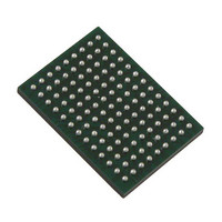
VSC8211XVW Vitesse Semiconductor Corp, VSC8211XVW Datasheet - Page 23

VSC8211XVW
Manufacturer Part Number
VSC8211XVW
Description
IC PHY 10/100/1000 SGL 117-LBGA
Manufacturer
Vitesse Semiconductor Corp
Type
PHY Transceiverr
Specifications of VSC8211XVW
Number Of Drivers/receivers
1/1
Protocol
Gigabit Ethernet
Voltage - Supply
3 V ~ 3.6 V
Mounting Type
Surface Mount
Package / Case
117-LBGA
Case
BGA
Dc
07+
Lead Free Status / RoHS Status
Lead free / RoHS Compliant
Other names
907-1023
Available stocks
Company
Part Number
Manufacturer
Quantity
Price
Company:
Part Number:
VSC8211XVW
Manufacturer:
VITESSE
Quantity:
5
Company:
Part Number:
VSC8211XVW
Manufacturer:
Semtech
Quantity:
3 413
Company:
Part Number:
VSC8211XVW
Manufacturer:
VITESSE
Quantity:
648
Company:
Part Number:
VSC8211XVW
Manufacturer:
Vitesse Semiconductor Corporation
Quantity:
10 000
Part Number:
VSC8211XVW
Manufacturer:
VITESSE
Quantity:
20 000
9.4.3 Analog Bias Signals
9.4.4 JTAG Access Port
VMDS-10105 Revision 4.1
October 2006
117 LBGA
117 LBGA
BALL
BALL
B10
A11
B11
H6
C9
C8
J6
Signal Name
Signal Name
REFREXT
REFFILT
TRST
TDO
TMS
TCK
TDI
A
A
I
I
I
I
Type
Type
O
PU5V
PU5V
PU5V
PU5V
BIAS
BIAS
ZC
REFREXT - Reference External Resistor.
Bias pin connects through external 2kΩ (1%) resistor to analog ground.
REFFILT - Reference Filter.
Filter internal reference through external 0.1μF (10%) capacitor to analog ground.
JTAG Test Data Serial Input Data.
Serial test pattern data is scanned into the device on this input pin, which is sam-
pled with respect to the rising edge of TCK.
This pin should be tied high to VDDIOCTRL in designs that do not require JTAG
functionality.
JTAG Test Data Serial Output Data.
Serial test data from the PHY is driven out of the device on the falling edge of
TCK. This pin should be left floating during normal chip operation.
JTAG Test Mode Select.
This input pin, sampled on the rising edge of TCK, controls the TAP (Test Access
Port) controller’s 16-state, instruction state machine.
This pin should be tied high to VDDIOCTRL in designs that do not require JTAG
functionality.
JTAG Test Clock.
This input pin is the master clock source used to control all JTAG test logic in the
device.
This pin should be pulled down with a 2kΩ pull-down resistor in designs that
require JTAG functionality.
This pin should be tied low in designs that do not require JTAG functionality.
JTAG Reset.
This active low input pin serves as an asynchronous reset to the JTAG TAP con-
troller’s state machine. As required by the JTAG standard, this pin includes an
integrated on-chip pull-up (to VDDIOCTRL) resistor. Because of the internal pull-
up, if the JTAG controller on the printed circuit board does not utilize the TRST sig-
nal, then the device will still function correctly when the TRST pin is left uncon-
nected on the board.
If the JTAG port of the PHY is not used on the printed circuit board, then this pin
should be pulled down with a 2kΩ pull-down resistor or a falling edge must be pro-
vided to this pin after PHY power up.
Table 4. Analog Bias Signals
Table 5. JTAG Access Port
23 of 165
Description
Description
Datasheet
VSC8211


