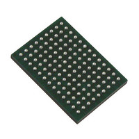
VSC8211XVW Vitesse Semiconductor Corp, VSC8211XVW Datasheet - Page 69

VSC8211XVW
Manufacturer Part Number
VSC8211XVW
Description
IC PHY 10/100/1000 SGL 117-LBGA
Manufacturer
Vitesse Semiconductor Corp
Type
PHY Transceiverr
Specifications of VSC8211XVW
Number Of Drivers/receivers
1/1
Protocol
Gigabit Ethernet
Voltage - Supply
3 V ~ 3.6 V
Mounting Type
Surface Mount
Package / Case
117-LBGA
Case
BGA
Dc
07+
Lead Free Status / RoHS Status
Lead free / RoHS Compliant
Other names
907-1023
Available stocks
Company
Part Number
Manufacturer
Quantity
Price
Company:
Part Number:
VSC8211XVW
Manufacturer:
VITESSE
Quantity:
5
Company:
Part Number:
VSC8211XVW
Manufacturer:
Semtech
Quantity:
3 413
Company:
Part Number:
VSC8211XVW
Manufacturer:
VITESSE
Quantity:
648
Company:
Part Number:
VSC8211XVW
Manufacturer:
Vitesse Semiconductor Corporation
Quantity:
10 000
Part Number:
VSC8211XVW
Manufacturer:
VITESSE
Quantity:
20 000
VMDS-10105 Revision 4.1
October 2006
Condition Parameter
Link/Activity and
Linkxxxx/Activity
behaviour
RGMII/RTBI
Transmit Path
Timing
Compensation[1:0]
RGMII/RTBI Receive
Path
Timing
Compensation[1:0]
Auto-negotiation
Advertisement
Control[1:0]
Flow Control[1:0]
PHY Operating
Name
CMODE7[1:0]
CMODE Pin Name and Bit
CMODE7[3]
CMODE5[3:2]
CMODE5[1:0]
CMODE3[0],CMODE4[1]
Table 27. PHY Operating Condition Parameter Description (continued)
Position
Value
This sets the LED behaviour by setting the default values of
27.2:1
1
0
Sets the RGMII/RTBI Transmit Path Timing compensation. This timing
compensation adds a configurable delay to the signal on the TXC pin.
These CMODE bits set the default value of
00
01
10
11
Sets the RGMII/RTBI Receive Path Timing compensation. This timing
compensation adds a configurable delay to the RXC signal internal to the
chip. These CMODE bits set the default value of
00
01
10
11
These CMODE bits set the default auto-negotiation advertisement by set-
ting the initial values of
00
01
10
11
00-11 Sets the default value of the Flow Control bits of MII Register 4.
69 of 165
.
Link function indicated link status only.
All link function blinks or flashes when activity is present. Blink or
flash behavior is selected by the Blink/Pulse-stretch Enable and
Blink/Pulse-stretch rate bits.
2.0ns
2.5ns
No skew
1.5ns
2.0ns
2.5ns
No skew
1.5ns
10/100/1000BASE-T HDX, 10/100/1000BASE-T FDX
10/100BASE-T HDX, 10/100/1000BASE-T FDX
10/100BASE-T HDX, 10/100BASE-T FDX
1000BASE-T FDX
The value on these CMODE pins is the default value of
ter 4.11:10
of
The MII Register View is set by CMODE bit CMODE4[0] (page 70).
MII Register 4.8:7
in Clause 28 Register View Mode and the default value
MII Registers 4
in Clause 37 Register View Mode.
Description
and 9.
MII Register
MII Register
23.11:10.
MII Register
23.9:8.
Datasheet
MII Regis-
VSC8211


