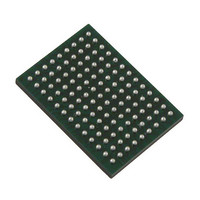
VSC8211XVW Vitesse Semiconductor Corp, VSC8211XVW Datasheet - Page 52

VSC8211XVW
Manufacturer Part Number
VSC8211XVW
Description
IC PHY 10/100/1000 SGL 117-LBGA
Manufacturer
Vitesse Semiconductor Corp
Type
PHY Transceiverr
Specifications of VSC8211XVW
Number Of Drivers/receivers
1/1
Protocol
Gigabit Ethernet
Voltage - Supply
3 V ~ 3.6 V
Mounting Type
Surface Mount
Package / Case
117-LBGA
Case
BGA
Dc
07+
Lead Free Status / RoHS Status
Lead free / RoHS Compliant
Other names
907-1023
Available stocks
Company
Part Number
Manufacturer
Quantity
Price
Company:
Part Number:
VSC8211XVW
Manufacturer:
VITESSE
Quantity:
5
Company:
Part Number:
VSC8211XVW
Manufacturer:
Semtech
Quantity:
3 413
Company:
Part Number:
VSC8211XVW
Manufacturer:
VITESSE
Quantity:
648
Company:
Part Number:
VSC8211XVW
Manufacturer:
Vitesse Semiconductor Corporation
Quantity:
10 000
Part Number:
VSC8211XVW
Manufacturer:
VITESSE
Quantity:
20 000
13.2 PHY Register Access with SMI in IEEE Mode
In IEEE mode, the SMI is fully compliant with the IEEE 802.3-2000 MII Interface specifications.
In IEEE mode, the SMI pins function as follows:
As many as 32 PHYs (32 distinct PHY Addresses) can share a common IEEE SMI signal pair (MDC, MDIO).
Data is transferred over the IEEE SMI using 32-bit frames with an optional and arbitrary length preamble. The IEEE SMI frame
format is described in the following table.
VMDS-10105 Revision 4.1
October 2006
# of bits
Read
Write
• Idle: During idle, the MDIO node goes to a high-impedance state. This allows an external pull-up resistor to
pull the MDIO node up to a logical “1” state. Since idle mode should not contain any transitions on MDIO, the
number of bits is undefined during idle.
• Preamble: For the VSC8211, the preamble is optional. By default, preambles are not expected or required.
The preamble is a string of “1”s. If it exists, the preamble must be at least one bit, but otherwise my be
arbitrarily long. See MII Register 1.6 for more information.
• Start of frame: A “01” pattern indicates the start of frame. If these bits are anything other than “01”, all
following bits are ignored until the next “preamble:0” pattern is detected.
• Operation code: A “10” pattern indicates a read. A “01” pattern indicates a write. If these bits are anything
other than “01” or “10”, all following bits are ignored until the next “preamble:0” pattern is detected.
• PHY address: The next five bits are the PHY address. The PHY responds to a message frame only when
the received PHY address matches its physical address. The PHY's address is indicated by the CMODE1[2]
and CMODE0[3:0] bits.
• Register address: The next five bits are the register address.
• Turn-around: The next two bits are “turn-around” (TA) bits. They are used to avoid contention when a read
operation is performed on the MDIO. During read operations, the VSC8211 will drive the second TA bit,
which is a logical “0”.
• Data: The next sixteen bits are data bits. When data is being read from the PHY, data is valid at the output
of the PHY from one rising edge of MDC to the next rising edge of MDC. When data is being written to the
PHY, data must be valid around the rising edge of MDC.
• Idle: The sequence is repeated.
MDC
MDIO
MDINT
Output
Input
Output
Input
Direction
VSC8211
from
Pin Name
1+
Z’s
1’s
Z’s
1’s
Preamble
2
ZZ
01
ZZ
01
Clock Input, 0 – 12.5 Mhz.
Bidirectional Data. This pin should be pulled high on the board using a 4.7kΩ to
10kΩ resistor.
Active Low or Active High open drain interrupt output.
Start of
Frame
Table 18. SMI Pin Descriptions - MSA Mode
Table 19. SMI Frame Format
2
ZZ
10
ZZ
01
Op Code
52 of 165
5
Z’s
addr
Z’s
addr
Address
PHY
Description
5
Z’s
addr
Z’s
addr
Register
Address
2
Z0
ZZ
ZZ
10
Around
Turn-
16
data
Z’s
Z’s
data
Data
Datasheet
Z’s
?
Z’s
Z’s
Z’s
VSC8211
Idle


