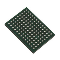
VSC8211XVW Vitesse Semiconductor Corp, VSC8211XVW Datasheet - Page 59

VSC8211XVW
Manufacturer Part Number
VSC8211XVW
Description
IC PHY 10/100/1000 SGL 117-LBGA
Manufacturer
Vitesse Semiconductor Corp
Type
PHY Transceiverr
Specifications of VSC8211XVW
Number Of Drivers/receivers
1/1
Protocol
Gigabit Ethernet
Voltage - Supply
3 V ~ 3.6 V
Mounting Type
Surface Mount
Package / Case
117-LBGA
Case
BGA
Dc
07+
Lead Free Status / RoHS Status
Lead free / RoHS Compliant
Other names
907-1023
Available stocks
Company
Part Number
Manufacturer
Quantity
Price
Company:
Part Number:
VSC8211XVW
Manufacturer:
VITESSE
Quantity:
5
Company:
Part Number:
VSC8211XVW
Manufacturer:
Semtech
Quantity:
3 413
Company:
Part Number:
VSC8211XVW
Manufacturer:
VITESSE
Quantity:
648
Company:
Part Number:
VSC8211XVW
Manufacturer:
Vitesse Semiconductor Corporation
Quantity:
10 000
Part Number:
VSC8211XVW
Manufacturer:
VITESSE
Quantity:
20 000
taken and examined. It also allows data values to be loaded into the boundary-scan cells prior to the selection of other
boundary-scan test instructions.
IDCODE
The optional IDCODE instruction provides the version number (bits 31:28), and Vitesse’s manufacturer identity (bits11:1), which
can be serially read from the PHY. See
PHY-specific values for this instruction.
CLAMP
The optional CLAMP instruction allows the state of the signals driven from the component pins to be determined from the
Boundary-Scan Register while the Bypass Register is selected as the serial path between TDI and TDO. While the CLAMP
instruction is selected, the signals driven from the component pins will not change.
HIGHZ
The optional HIGHZ instruction places the component in a state in which all of its system logic outputs are placed in a high
impedance state. In this state, an in-circuit test system may drive signals onto the connections normally driven by a component
output without incurring a risk of damage to the component. This makes it possible to use a board where not all of the
components are compatible with the IEEE 1149.1 standard.
BYPASS
The Bypass Register contains a single shift-register stage and is used to provide a minimum-length serial path (one TCK clock
period) between TDI and TDO to bypass the device when no test operation is required.
15.2 Boundary-Scan Register Cell Order
All inputs and outputs are observed in the Boundary-Scan Register cells. All outputs are additionally driven by the contents of
Boundary-Scan Register cells. Bidirectional pins have all three related Boundary-Scan Register cells: the input, the output, and
the control. The full boundary scan cell order is available from Vitesse Semiconductor in *.BSD file format.
1
VMDS-10105 Revision 4.1
October 2006
Following the use of this instruction, the on-chip system logic may be in an indeterminate state that will persist until a system reset is applied.
Therefore, the on-chip system logic may need to be reset on return to normal (i.e., non-test) operation.
“Register 3 (03h) – PHY Identifier Register #2 - Clause 28/37 View”
59 of 165
1
1
on page 88 for the
Datasheet
VSC8211


