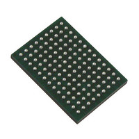
VSC8211XVW Vitesse Semiconductor Corp, VSC8211XVW Datasheet - Page 27

VSC8211XVW
Manufacturer Part Number
VSC8211XVW
Description
IC PHY 10/100/1000 SGL 117-LBGA
Manufacturer
Vitesse Semiconductor Corp
Type
PHY Transceiverr
Specifications of VSC8211XVW
Number Of Drivers/receivers
1/1
Protocol
Gigabit Ethernet
Voltage - Supply
3 V ~ 3.6 V
Mounting Type
Surface Mount
Package / Case
117-LBGA
Case
BGA
Dc
07+
Lead Free Status / RoHS Status
Lead free / RoHS Compliant
Other names
907-1023
Available stocks
Company
Part Number
Manufacturer
Quantity
Price
Company:
Part Number:
VSC8211XVW
Manufacturer:
VITESSE
Quantity:
5
Company:
Part Number:
VSC8211XVW
Manufacturer:
Semtech
Quantity:
3 413
Company:
Part Number:
VSC8211XVW
Manufacturer:
VITESSE
Quantity:
648
Company:
Part Number:
VSC8211XVW
Manufacturer:
Vitesse Semiconductor Corporation
Quantity:
10 000
Part Number:
VSC8211XVW
Manufacturer:
VITESSE
Quantity:
20 000
1
VMDS-10105 Revision 4.1
October 2006
LBGA
BALL
See
117
B3
A2
TX_CLK
PMAT
XCLK
TX[9]
TBI
pin description in following section.
Parallel MAC Interface Modes
TD[9]
TD[4]
RTBI
TXC
and
Table 9. Parallel MAC Interface Signals - Transmit Signals (continued)
Signal Name
GTXCLK
TXER
GMII
TXER
used
Not
MII
1
TXCTL
RGMII
TXC
Type
27 of 165
I
I
PD
PD
Transmit Data Input (TBI mode).
Transmit code-group data bit 9 is input on this pin synchro-
nously to the rising edge of PMATXCLK in TBI mode.
Multiplexed Transmit Data Input (RTBI mode).
Bit [4] is synchronously input on the rising edge of TXC, and
bit [9] on the falling edge of TXC.
Transmit Error Input (GMII, MII modes).
When asserted, this synchronous input causes error sym-
bols to be transmitted from the PHY when operating in
100Mb or 1000Mb modes.
Transmit Enable, Transmit Error Multiplexed Input
(RGMII mode).
In RGMII mode, this input is sampled by the PHY on oppo-
site edges of TXC to indicate two transmit conditions of the
MAC:
1) on the rising edge of TXC, this input serves as TXEN, indi-
cating valid data is available on the TD input data bus.
2) on the falling edge of TXC, this input signals a transmit
error from the MAC, based on a logical derivative of TXEN
and TXER, per RGMII specification Version 1.2a, Section
3.4.
PMA Transmit Code Group Clock Input (TBI mode).
125 MHz transmit code-group clock. This code-group clock
is used to latch data into the PMA (in this case, the PHY) for
transmission.
Transmit Clock Input (GMII mode).
The transmit clock GTXCLK is a 125MHz, +/-100ppm refer-
ence clock used to synchronize the TXD data code group,
TXD[7:0], into the PHY.
Transmit Clock Input (RGMII/RTBI mode).
The transmit clock shall be either a 125MHz or 25MHz (for
1000Mb or 100Mb modes, respectively), with a +/-50ppm tol-
erance.
Description
Datasheet
VSC8211


