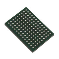
VSC8211XVW Vitesse Semiconductor Corp, VSC8211XVW Datasheet - Page 30

VSC8211XVW
Manufacturer Part Number
VSC8211XVW
Description
IC PHY 10/100/1000 SGL 117-LBGA
Manufacturer
Vitesse Semiconductor Corp
Type
PHY Transceiverr
Specifications of VSC8211XVW
Number Of Drivers/receivers
1/1
Protocol
Gigabit Ethernet
Voltage - Supply
3 V ~ 3.6 V
Mounting Type
Surface Mount
Package / Case
117-LBGA
Case
BGA
Dc
07+
Lead Free Status / RoHS Status
Lead free / RoHS Compliant
Other names
907-1023
Available stocks
Company
Part Number
Manufacturer
Quantity
Price
Company:
Part Number:
VSC8211XVW
Manufacturer:
VITESSE
Quantity:
5
Company:
Part Number:
VSC8211XVW
Manufacturer:
Semtech
Quantity:
3 413
Company:
Part Number:
VSC8211XVW
Manufacturer:
VITESSE
Quantity:
648
Company:
Part Number:
VSC8211XVW
Manufacturer:
Vitesse Semiconductor Corporation
Quantity:
10 000
Part Number:
VSC8211XVW
Manufacturer:
VITESSE
Quantity:
20 000
9.4.10 Serial MAC/Media Interface Signals
VMDS-10105 Revision 4.1
October 2006
LBGA
BALL
117
LBGA
C4
B4
BALL
117
H2
H1
J3
J4
RXCLK
COM-
DET
TBI
125
Signal
Name
TDN
RDP
RDN
TDP
Parallel MAC Interface Modes
uncon-
nected
uncon-
nected
Leave
Leave
RTBI
pins
pins
Table 10. Parallel MAC Interface Signals - Receive Signals (continued)
Signal Name
O
Type
I
DIFF
DIFF
GMII
CRS
COL
Transmitter Data Differential Input Pair (used in SerDes/SGMII to CAT5 and Parallel
MAC to SerDes/AMS PHY Operating Modes).
Differential 1.25Gbaud receiver inputs with register selectable on-chip 100Ω or 150Ω dif-
ferential termination. The TDP and TDN signals should be AC-coupled with external
0.01μF series capacitors. See
Receiver Data Differential Output Pair (used in SerDes/SGMII to CAT5 and Parallel
MAC to SerDes/AMS PHY Operating Modes).
Differential 1.25Gbaud transmitter outputs. External 0.01μF AC coupling capacitors
should be located on the PHY side. The register selectable 100Ω or 150Ω differential ter-
mination should be placed near the MAC side. See
further information. For information about adjusting the output swing of these pins, see
Register 17E (11h) – SerDes Control
Table 11. Serial MAC/Media Interface Signals
CRS
COL
MII
uncon-
uncon-
RGMII
nected
nected
Leave
Leave
pins
pins
Type
O
O
30 of 165
ZC
ZC
Comma Detect Output (TBI mode).
A high on this signal indicates that the code-group associated
with the current PMARXCLK1 contains a valid comma. In TBI
mode, the PHY detects and code-group-aligns to the
comma+ bit sequence.
Carrier Sense Output (GMII, MII modes).
Valid only in GMII and MII half duplex modes, CRS is
asserted high when a valid carrier is detected on the media.
Collision Detect Output (GMII, MII modes).
This output is asserted high when a collision is detected on
the media. For full-duplex modes, this output is always low.
Receiver Clock 125MHz Output (TBI mode).
This signal behaves differently, depending on whether TBI
loopback mode is enabled:
When switching from one of these three operating modes to
another, RXCLK125’s low time will be extended, if necessary,
to avoid clock glitching.
Section 10: “System Schematics”
1) When TBI loopback mode is enabled, RXCLK125
2) When no carrier is present on the media, this signal is
3) When a valid carrier is detected on the media, this out-
becomes one-half the frequency of the GTXCLK input
clock from the protocol device (or MAC).
the same as the device’s free running output clock sig-
nal, CLKOUTMAC.
put signal is the recovered clock from the TBI’s data
stream.
Register, page 124.
Description
Section 10: “System Schematics”
Description
for further information.
Datasheet
VSC8211
for


