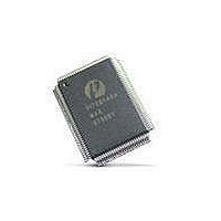
PI7C8140AMAE Pericom Semiconductor, PI7C8140AMAE Datasheet - Page 17

PI7C8140AMAE
Manufacturer Part Number
PI7C8140AMAE
Description
IC PCI-PCI BRIDGE 2PORT 128-QFP
Manufacturer
Pericom Semiconductor
Datasheet
1.PI7C8140AMAE.pdf
(82 pages)
Specifications of PI7C8140AMAE
Applications
*
Interface
*
Voltage - Supply
*
Package / Case
128-QFP
Mounting Type
Surface Mount
Maximum Operating Temperature
+ 85 C
Minimum Operating Temperature
0 C
Mounting Style
SMD/SMT
Operating Supply Voltage
3 V to 3.6 V
Supply Current (max)
230 mA
Lead Free Status / RoHS Status
Lead free / RoHS Compliant
Available stocks
Company
Part Number
Manufacturer
Quantity
Price
Company:
Part Number:
PI7C8140AMAE
Manufacturer:
Pericom
Quantity:
135
Company:
Part Number:
PI7C8140AMAE
Manufacturer:
SONY
Quantity:
469
Part Number:
PI7C8140AMAE
Manufacturer:
PERICOM
Quantity:
20 000
07-0067
2.2
2.3
2.4
2.5
SINGLE ADDRESS PHASE
A 32-bit address uses a single address phase. This address is driven on P_AD[31:0], and the bus
command is driven on P_CBE[3:0]. The bridge supports the linear increment address mode only, which
is indicated when the lowest two address bits are equal to zero. If either of the lowest two address bits is
nonzero, the bridge automatically disconnects the transaction after the first data transfer.
DEVICE SELECT (DEVSEL#) GENERATION
The bridge always performs positive address decoding (medium decode) when accepting transactions
on either the primary or secondary buses. The bridge never does subtractive decode.
DATA PHASE
The address phase of a PCI transaction is followed by one or more data phases. A data phase is
completed when IRDY# and either TRDY# or STOP# are asserted. A transfer of data occurs only
when both IRDY# and TRDY# are asserted during the same PCI clock cycle. The last data phase of a
transaction is indicated when FRAME# is de-asserted and both TRDY# and IRDY# are asserted, or
when IRDY# and STOP# are asserted. See Section 2.8 for further discussion of transaction termination.
Depending on the command type, the bridge can support multiple data phase PCI transactions. For
detailed descriptions of how the bridge imposes disconnect boundaries, see Section 2.5.4 for write
address boundaries and Section 2.6.4 read address boundaries.
WRITE TRANSACTIONS
Write transactions are treated as either posted write or delayed write transactions. Table 2-2 shows the
method of forwarding used for each type of write operation.
Table 2-2. Write Transaction Forwarding
Type of Transaction
Memory Write
Memory Write and Invalidate
Memory Write to VGA memory
I/O Write
Type 1 Configuration Write
The bridge does not respond to special cycle transactions. The bridge cannot guarantee delivery of
a special cycle transaction to downstream buses because of the broadcast nature of the special cycle
command and the inability to control the transaction as a target. To generate special cycle
transactions on other PCI buses, either upstream or downstream, Type 1 configuration write must
be used.
The bridge neither generates Type 0 configuration transactions on the primary PCI bus nor
responds to Type 0 configuration transactions on the secondary PCI buses.
Page 17 of 82
Type of Forwarding
Posted (except VGA memory)
Posted
Delayed
Delayed
Delayed
2-PORT PCI-TO-PCI BRIDGE
March 20, 2007 – Revision 1.01
PI7C8140A


