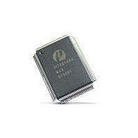
PI7C8140AMAE Pericom Semiconductor, PI7C8140AMAE Datasheet - Page 37

PI7C8140AMAE
Manufacturer Part Number
PI7C8140AMAE
Description
IC PCI-PCI BRIDGE 2PORT 128-QFP
Manufacturer
Pericom Semiconductor
Datasheet
1.PI7C8140AMAE.pdf
(82 pages)
Specifications of PI7C8140AMAE
Applications
*
Interface
*
Voltage - Supply
*
Package / Case
128-QFP
Mounting Type
Surface Mount
Maximum Operating Temperature
+ 85 C
Minimum Operating Temperature
0 C
Mounting Style
SMD/SMT
Operating Supply Voltage
3 V to 3.6 V
Supply Current (max)
230 mA
Lead Free Status / RoHS Status
Lead free / RoHS Compliant
Available stocks
Company
Part Number
Manufacturer
Quantity
Price
Company:
Part Number:
PI7C8140AMAE
Manufacturer:
Pericom
Quantity:
135
Company:
Part Number:
PI7C8140AMAE
Manufacturer:
SONY
Quantity:
469
Part Number:
PI7C8140AMAE
Manufacturer:
PERICOM
Quantity:
20 000
07-0067
3.4 VGA SUPPORT
3.4.1 VGA MODE
Prefetchable memory address range has a granularity and alignment of 1MB. Maximum memory
address range is 4GB when 32-bit addressing is being used. Prefetchable memory address range is
defined by a 16-bit prefetchable memory base address register at configuration offset 24h and by a 16-
bit prefetchable memory limit address register at offset 26h. The top 12 bits of each of these registers
correspond to bits [31:20] of the memory address. The lowest 4 bits are hardwired to 1h. The lowest 20
bits of the prefetchable memory base address are assumed to be 0 0000h, which results in a natural
alignment to a 1MB boundary. The lowest 20 bits of the prefetchable memory limit address are
assumed to be FFFFFh, which results in an alignment to the top of a 1MB block.
Note: The initial state of the prefetchable memory base address register is 0000 0000h. The initial state
of the prefetchable memory limit address register is 000F FFFFh. Note that the initial states of these
registers define a prefetchable memory range at the bottom 1MB block of memory. Write these
registers with their appropriate values before setting either the memory enable bit or the master enable
bit in the command register in configuration space.
To turn off the prefetchable memory address range, write the prefetchable memory base address register
with a value greater than that of the prefetchable memory limit address register. The entire base value
must be greater than the entire limit value, meaning that the upper 32 bits must be considered.
Therefore, to disable the address range, the upper 32 bits registers can both be set to the same value,
while the lower base register is set greater than the lower limit register. Otherwise, the upper 32-bit base
must be greater than the upper 32-bit limit.
The bridge provides two modes for VGA support:
When a VGA-compatible device exists downstream from the bridge, set the VGA mode bit in the
bridge control register in configuration space to enable VGA mode. When the bridge is operating in
VGA mode, it forwards downstream those transactions addressing the VGA frame buffer memory and
VGA I/O registers, regardless of the values of the base and limit address registers. The bridge ignores
transactions initiated on the secondary interface addressing these locations.
The VGA frame buffer consists of the following memory address range:
000A 0000h–000B FFFFh
Read transactions to frame buffer memory are treated as non-prefetchable. The bridge requests only a
single data transfer from the target, and read byte enable bits are forwarded to the target bus.
The VGA I/O addresses are in the range of 3B0h–3BBh and 3C0h–3DFh I/O. These I/O addresses are
aliases every 1KB throughout the first 64KB of I/O space. This means that address bits <15:10> are not
decoded and can be any value, while address bits [31:16] must be all 0’s. VGA BIOS addresses starting
at C0000h are not decoded in VGA mode.
VGA mode, supporting VGA-compatible addressing
VGA snoop mode, supporting VGA palette forwarding
Page 37 of 82
2-PORT PCI-TO-PCI BRIDGE
March 20, 2007 – Revision 1.01
PI7C8140A


