MA180023 Microchip Technology, MA180023 Datasheet - Page 132
MA180023
Manufacturer Part Number
MA180023
Description
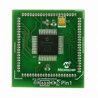
MODULE PLUG-IN PIC18F46J11 PIM
Manufacturer
Microchip Technology
Series
PIC®r
Datasheet
1.MA180023.pdf
(528 pages)
Specifications of MA180023
Accessory Type
Plug-In Module (PIM) - PIC18F46J11
Tool / Board Applications
General Purpose MCU, MPU, DSP, DSC
Mcu Supported Families
PIC18
Supported Devices
Stand-alone Or W/ HPC(DM183022) Or PIC18(DM183032)
Silicon Manufacturer
Microchip
Core Architecture
PIC
Core Sub-architecture
PIC18
Silicon Core Number
PIC18F
Silicon Family Name
PIC18FxxJxx
Lead Free Status / RoHS Status
Lead free / RoHS Compliant
For Use With/related Products
HPC Explorer Board (DM183022) or PIC18 Explorer Board (DM183032)
For Use With
DM183032 - BOARD EXPLORER PICDEM PIC18DM183022 - BOARD DEMO PIC18FXX22 64/80TQFP
Lead Free Status / RoHS Status
Lead free / RoHS Compliant
Available stocks
Company
Part Number
Manufacturer
Quantity
Price
Company:

Part Number:
MA180023
Manufacturer:
Microchip Technology
Quantity:
135


PIC18F46J11 FAMILY
9.3
PORTB is an 8-bit wide, bidirectional port. The corre-
sponding Data Direction register is TRISB. Setting a
TRISB bit (= 1) will make the corresponding PORTB
pin an input (i.e., put the corresponding output driver in
a high-impedance mode). Clearing a TRISB bit (= 0)
will make the corresponding PORTB pin an output (i.e.,
put the contents of the output latch on the selected pin).
The Data Latch register (LATB) is also memory
mapped. Read-modify-write operations on the LATB
register read and write the latched output value for
PORTB.
EXAMPLE 9-3:
Each of the PORTB pins has a weak internal pull-up. A
single control bit can turn on all the pull-ups. This is
performed by clearing bit, RBPU (INTCON2<7>). The
weak pull-up is automatically turned off when the port
pin is configured as an output. The pull-ups are
disabled on a POR.
DS39932C-page 132
CLRF
CLRF
MOVLW 0x3F
MOVFF WREG ADCON1 ; pins in this example
MOVLW 0CFh
MOVWF TRISB
Note:
PORTB
LATB
PORTB, TRISB and LATB
Registers
On a POR, the RB<3:0> bits are
configured as analog inputs by default and
read as ‘0’; RB<7:4> bits are configured
as digital inputs.
; Initialize PORTB by
; clearing output
; data latches
; Alternate method
; to clear output
; data latches
; Configure as digital I/O
; Value used to
; initialize data
; direction
; Set RB<3:0> as inputs
; RB<5:4> as outputs
; RB<7:6> as inputs
INITIALIZING PORTB
Four of the PORTB pins (RB<7:4>) have an interrupt-
on-change feature. Only pins configured as inputs can
cause this interrupt to occur (i.e., any RB<7:4> pin
configured as an output is excluded from the interrupt-
on-change comparison). The input pins (of RB<7:4>)
are compared with the old value latched on the last
read of PORTB. The “mismatch” outputs of RB<7:4>
are ORed together to generate the RB Port Change
Interrupt with Flag bit, RBIF (INTCON<0>).
This interrupt can wake the device from Sleep mode or
any of the Idle modes. The user, in the Interrupt Service
Routine (ISR), can clear the interrupt using the following
steps:
1.
2.
3.
A mismatch condition continues to set flag bit, RBIF.
Reading PORTB will end the mismatch condition and
allow flag bit, RBIF, to be cleared after one instruction
cycle of delay.
The interrupt-on-change feature is recommended for
wake-up on key depression operation and operations
where PORTB is only used for the interrupt-on-change
feature. Polling of PORTB is not recommended while
using the interrupt-on-change feature.
The RB5 pin is multiplexed with the Timer0 module
clock input and one of the comparator outputs to
become the RB5/KBI1/SDI1/SDA1/RP8 pin.
Any read or write of PORTB (except with the
MOVFF (ANY), PORTB instruction).
Wait one instruction cycle (such as executing a
NOP instruction).
Clear flag bit, RBIF.
© 2009 Microchip Technology Inc.
Related parts for MA180023
Image
Part Number
Description
Manufacturer
Datasheet
Request
R

Part Number:
Description:
Manufacturer:
Microchip Technology Inc.
Datasheet:
Part Number:
Description:
Manufacturer:
Microchip Technology Inc.
Datasheet:
Part Number:
Description:
Manufacturer:
Microchip Technology Inc.
Datasheet:
Part Number:
Description:
Manufacturer:
Microchip Technology Inc.
Datasheet:
Part Number:
Description:
Manufacturer:
Microchip Technology Inc.
Datasheet:
Part Number:
Description:
Manufacturer:
Microchip Technology Inc.
Datasheet:
Part Number:
Description:
Manufacturer:
Microchip Technology Inc.
Datasheet:
Part Number:
Description:
Manufacturer:
Microchip Technology Inc.
Datasheet: