MA180023 Microchip Technology, MA180023 Datasheet - Page 37
MA180023
Manufacturer Part Number
MA180023
Description
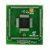
MODULE PLUG-IN PIC18F46J11 PIM
Manufacturer
Microchip Technology
Series
PIC®r
Datasheet
1.MA180023.pdf
(528 pages)
Specifications of MA180023
Accessory Type
Plug-In Module (PIM) - PIC18F46J11
Tool / Board Applications
General Purpose MCU, MPU, DSP, DSC
Mcu Supported Families
PIC18
Supported Devices
Stand-alone Or W/ HPC(DM183022) Or PIC18(DM183032)
Silicon Manufacturer
Microchip
Core Architecture
PIC
Core Sub-architecture
PIC18
Silicon Core Number
PIC18F
Silicon Family Name
PIC18FxxJxx
Lead Free Status / RoHS Status
Lead free / RoHS Compliant
For Use With/related Products
HPC Explorer Board (DM183022) or PIC18 Explorer Board (DM183032)
For Use With
DM183032 - BOARD EXPLORER PICDEM PIC18DM183022 - BOARD DEMO PIC18FXX22 64/80TQFP
Lead Free Status / RoHS Status
Lead free / RoHS Compliant
Available stocks
Company
Part Number
Manufacturer
Quantity
Price
Company:

Part Number:
MA180023
Manufacturer:
Microchip Technology
Quantity:
135


2.3.1
The OSCCON register (Register 2-2) controls several
aspects of the device clock’s operation, both in
full-power operation and in power-managed modes.
The System Clock Select bits, SCS<1:0>, select the
clock source. The available clock sources are the
primary clock (defined by the FOSC<2:0> Configura-
tion bits), the secondary clock (Timer1 oscillator) and
the postscaled internal clock.The clock source changes
immediately, after one or more of the bits is written to,
following a brief clock transition interval. The SCS bits
are cleared on all forms of Reset.
The
IRCF<2:0>, select the frequency output provided on the
postscaled internal clock line. The choices are the
INTRC source, the INTOSC source (8 MHz) or one of
the frequencies derived from the INTOSC postscaler
(31 kHz to 4 MHz). If the postscaled internal clock is
supplying the device clock, changing the states of these
bits will have an immediate change on the internal oscil-
lator’s output. On device Resets, the default output
frequency of the INTOSC postscaler is set at 4 MHz.
When an output frequency of 31 kHz is selected
(IRCF<2:0> = 000), users may choose the internal
oscillator, which acts as the source. This is done with
the
(OSCTUNE<7>). Setting this bit selects INTOSC as a
31.25 kHz clock source by enabling the divide-by-256
output of the INTOSC postscaler. Clearing INTSRC
selects INTRC (nominally 31 kHz) as the clock source.
This option allows users to select the tunable and more
precise INTOSC as a clock source, while maintaining
power savings with a very low clock speed. Regardless
of the setting of INTSRC, INTRC always remains the
clock source for features such as the WDT and the
FSCM.
The OSTS and T1RUN bits indicate which clock source
is currently providing the device clock. The OSTS bit
indicates that the Oscillator Start-up Timer (OST) has
timed out and the primary clock is providing the device
clock in primary clock modes. The T1RUN bit
(T1CON<6>) indicates when the Timer1 oscillator is
providing the device clock in secondary clock modes.
In power-managed modes, only one of these bits will
be set at any time. If none of these bits are set, the
INTRC is providing the clock or the internal oscillator
block has just started and is not yet stable.
© 2009 Microchip Technology Inc.
INTSRC
Internal
OSCILLATOR CONTROL REGISTER
Oscillator
bit
in
the
Frequency
OSCTUNE
Select
register
bits,
PIC18F46J11 FAMILY
The IDLEN bit determines if the device goes into Sleep
mode, or one of the Idle modes, when the SLEEP
instruction is executed.
The use of the flag and control bits in the OSCCON
register is discussed in more detail in Section 3.0
“Low-Power Modes”.
2.3.2
PIC18F46J11 family devices contain circuitry to
prevent clock “glitches” when switching between clock
sources. A short pause in the device clock occurs dur-
ing the clock switch. The length of this pause is the sum
of two cycles of the old clock source and three to four
cycles of the new clock source. This formula assumes
that the new clock source is stable.
Clock transitions are discussed in more detail in
Section 3.1.2 “Entering Power-Managed Modes”.
Note 1: The Timer1 crystal driver is enabled by
2: If Timer1 is driving a crystal, it is recom-
OSCILLATOR TRANSITIONS
setting the T1OSCEN bit in the Timer1
Control register (T1CON<3>). If the
Timer1 oscillator is not enabled, then any
attempt to select the Timer1 clock source
will be ignored, unless the CONFIG2L
register’s T1DIG bit is set.
mended that the Timer1 oscillator be
operating and stable prior to switching to
it as the clock source; otherwise, a very
long delay may occur while the Timer1
oscillator starts.
DS39932C-page 37
Related parts for MA180023
Image
Part Number
Description
Manufacturer
Datasheet
Request
R

Part Number:
Description:
Manufacturer:
Microchip Technology Inc.
Datasheet:
Part Number:
Description:
Manufacturer:
Microchip Technology Inc.
Datasheet:
Part Number:
Description:
Manufacturer:
Microchip Technology Inc.
Datasheet:
Part Number:
Description:
Manufacturer:
Microchip Technology Inc.
Datasheet:
Part Number:
Description:
Manufacturer:
Microchip Technology Inc.
Datasheet:
Part Number:
Description:
Manufacturer:
Microchip Technology Inc.
Datasheet:
Part Number:
Description:
Manufacturer:
Microchip Technology Inc.
Datasheet:
Part Number:
Description:
Manufacturer:
Microchip Technology Inc.
Datasheet: