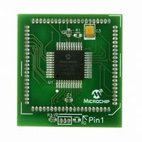
MA180023 Microchip Technology, MA180023 Datasheet - Page 192

MA180023
Manufacturer Part Number
MA180023
Description
MODULE PLUG-IN PIC18F46J11 PIM
Manufacturer
Microchip Technology
Series
PIC®r
Datasheet
1.MA180023.pdf
(528 pages)
Specifications of MA180023
Accessory Type
Plug-In Module (PIM) - PIC18F46J11
Tool / Board Applications
General Purpose MCU, MPU, DSP, DSC
Mcu Supported Families
PIC18
Supported Devices
Stand-alone Or W/ HPC(DM183022) Or PIC18(DM183032)
Silicon Manufacturer
Microchip
Core Architecture
PIC
Core Sub-architecture
PIC18
Silicon Core Number
PIC18F
Silicon Family Name
PIC18FxxJxx
Lead Free Status / RoHS Status
Lead free / RoHS Compliant
For Use With/related Products
HPC Explorer Board (DM183022) or PIC18 Explorer Board (DM183032)
For Use With
DM183032 - BOARD EXPLORER PICDEM PIC18DM183022 - BOARD DEMO PIC18FXX22 64/80TQFP
Lead Free Status / RoHS Status
Lead free / RoHS Compliant
Available stocks
Company
Part Number
Manufacturer
Quantity
Price
Company:
Part Number:
MA180023
Manufacturer:
Microchip Technology
Quantity:
135
- Current page: 192 of 528
- Download datasheet (8Mb)
PIC18F46J11 FAMILY
11.1
Timer0 can operate as either a timer or a counter. The
mode is selected with the T0CS bit (T0CON<5>). In
Timer mode (T0CS = 0), the module increments on
every clock by default unless a different prescaler value
is selected (see Section 11.3 “Prescaler”). If the
TMR0 register is written to, the increment is inhibited
for the following two instruction cycles. The user can
work around this by writing an adjusted value to the
TMR0 register.
The Counter mode is selected by setting the T0CS bit
(= 1). In this mode, Timer0 increments either on every
rising edge or falling edge of pin, T0CKI. The
incrementing edge is determined by the Timer0 Source
Edge Select bit, T0SE (T0CON<4>); clearing this bit
selects the rising edge. Restrictions on the external
clock input are discussed below.
An external clock source can be used to drive Timer0;
however, it must meet certain requirements to ensure
that the external clock can be synchronized with the
FIGURE 11-1:
FIGURE 11-2:
DS39932C-page 192
Note: Upon Reset, Timer0 is enabled in 8-bit mode with clock input from T0CKI max. prescale.
T0CKI pin
Note: Upon Reset, Timer0 is enabled in 8-bit mode with clock input from T0CKI max. prescale.
T0CKI pin
Timer0 Operation
T0SE
T0CS
T0PS<2:0>
PSA
F
OSC
T0SE
T0CS
T0PS<2:0>
PSA
/4
F
OSC
TIMER0 BLOCK DIAGRAM (8-BIT MODE)
TIMER0 BLOCK DIAGRAM (16-BIT MODE)
/4
0
1
0
1
Programmable
Prescaler
Programmable
3
Prescaler
3
1
0
1
0
(2 T
Sync with
Internal
Clocks
CY
(2 T
Delay)
Sync with
Internal
Clocks
CY
internal phase clock (T
synchronization and the onset of incrementing the
timer/counter.
11.2
TMR0H is not the actual high byte of Timer0 in 16-bit
mode. It is actually a buffered version of the real high
byte of Timer0, which is not directly readable nor
writable (refer to Figure 11-2). TMR0H is updated with
the contents of the high byte of Timer0 during a read of
TMR0L. This provides the ability to read all 16 bits of
Timer0 without having to verify that the read of the high
and low byte were valid, due to a rollover between
successive reads of the high and low byte.
Similarly, a write to the high byte of Timer0 must also
take place through the TMR0H Buffer register. The high
byte is updated with the contents of TMR0H when a
write occurs to TMR0L. This allows all 16 bits of Timer0
to be updated at once.
Delay)
Timer0 Reads and Writes in 16-Bit
Mode
TMR0L
8
8
TMR0L
8
8
OSC
© 2009 Microchip Technology Inc.
High Byte
TMR0H
TMR0
8
). There is a delay between
8
Set
TMR0IF
on Overflow
Internal Data Bus
8
Set
TMR0IF
on Overflow
Read TMR0L
Write TMR0L
Internal Data Bus
Related parts for MA180023
Image
Part Number
Description
Manufacturer
Datasheet
Request
R

Part Number:
Description:
Manufacturer:
Microchip Technology Inc.
Datasheet:

Part Number:
Description:
Manufacturer:
Microchip Technology Inc.
Datasheet:

Part Number:
Description:
Manufacturer:
Microchip Technology Inc.
Datasheet:

Part Number:
Description:
Manufacturer:
Microchip Technology Inc.
Datasheet:

Part Number:
Description:
Manufacturer:
Microchip Technology Inc.
Datasheet:

Part Number:
Description:
Manufacturer:
Microchip Technology Inc.
Datasheet:

Part Number:
Description:
Manufacturer:
Microchip Technology Inc.
Datasheet:

Part Number:
Description:
Manufacturer:
Microchip Technology Inc.
Datasheet:


