MA180023 Microchip Technology, MA180023 Datasheet - Page 345
MA180023
Manufacturer Part Number
MA180023
Description
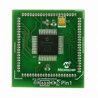
MODULE PLUG-IN PIC18F46J11 PIM
Manufacturer
Microchip Technology
Series
PIC®r
Datasheet
1.MA180023.pdf
(528 pages)
Specifications of MA180023
Accessory Type
Plug-In Module (PIM) - PIC18F46J11
Tool / Board Applications
General Purpose MCU, MPU, DSP, DSC
Mcu Supported Families
PIC18
Supported Devices
Stand-alone Or W/ HPC(DM183022) Or PIC18(DM183032)
Silicon Manufacturer
Microchip
Core Architecture
PIC
Core Sub-architecture
PIC18
Silicon Core Number
PIC18F
Silicon Family Name
PIC18FxxJxx
Lead Free Status / RoHS Status
Lead free / RoHS Compliant
For Use With/related Products
HPC Explorer Board (DM183022) or PIC18 Explorer Board (DM183032)
For Use With
DM183032 - BOARD EXPLORER PICDEM PIC18DM183022 - BOARD DEMO PIC18FXX22 64/80TQFP
Lead Free Status / RoHS Status
Lead free / RoHS Compliant
Available stocks
Company
Part Number
Manufacturer
Quantity
Price
Company:

Part Number:
MA180023
Manufacturer:
Microchip Technology
Quantity:
135


20.0
The Analog-to-Digital (A/D) Converter module has
10 inputs for the 28-pin devices and 13 for the 44-pin
devices. Additionally, two internal channels are
available for sampling the V
reference voltage. This module allows conversion of an
analog input signal to a corresponding 10-bit digital
number.
The module has six registers:
• A/D Control Register 0 (ADCON0)
REGISTER 20-1:
© 2009 Microchip Technology Inc.
bit 7
Legend:
R = Readable bit
-n = Value at POR
bit 7
bit 6
bit 5-2
bit 1
bit 0
Note 1:
VCFG1
R/W-0
2:
3:
10-BIT ANALOG-TO-DIGITAL
CONVERTER (A/D) MODULE
These channels are not implemented on 28-pin devices.
Performing a conversion on unimplemented channels will return random values.
For best accuracy, the band gap reference circuit should be enabled (ANCON1<7> = 1) at least 10 ms
before performing a conversion on this channel.
VCFG1: Voltage Reference Configuration bit (V
1 = V
0 = AV
VCFG0: Voltage Reference Configuration bit (V
1 = V
0 = AV
CHS<3:0>: Analog Channel Select bits
0000 = Channel 00 (AN0)
0001 = Channel 01 (AN1)
0010 = Channel 02 (AN2)
0011 = Channel 03 (AN3)
0100 = Channel 04 (AN4)
0101 = Channel 05 (AN5)
0110 = Channel 06 (AN6)
0111 = Channel 07 (AN7)
1000 = Channel 08 (AN8)
1001 = Channel 09 (AN9)
1010 = Channel 10 (AN10)
1011 = Channel 11 (AN11)
1100 = Channel 12 (AN12)
1101 = (Reserved)
1110 = V
1111 = V
GO/DONE: A/D Conversion Status bit
When ADON = 1:
1 = A/D conversion in progress
0 = A/D Idle
ADON: A/D On bit
1 = A/D Converter module is enabled
0 = A/D Converter module is disabled
VCFG0
R/W-0
REF
REF
SS
DD
ADCON0: A/D CONTROL REGISTER 0 (ACCESS FC2h)
- (AN2)
+ (AN3)
DDCORE
BG
DDCORE
Absolute Reference (~1.2V)
W = Writable bit
‘1’ = Bit is set
CHS3
R/W-0
and V
(2)
(1)
(1)
(1)
BG
absolute
CHS2
R/W-0
(2)
(2)
(3)
U = Unimplemented bit, read as ‘0’
‘0’ = Bit is cleared
PIC18F46J11 FAMILY
CHS1
REF
REF
R/W-0
• A/D Control Register 1 (ADCON1)
• A/D Port Configuration Register 2 (ANCON0)
• A/D Port Configuration Register 1 (ANCON1)
• A/D Result Registers (ADRESH and ADRESL)
The ADCON0 register, in Register 20-1, controls the
operation of the A/D module. The ADCON1 register, in
Register 20-2, configures the A/D clock source,
programmed acquisition time and justification.
The ANCON0 and ANCON1 registers, in Register 20-3
and Register 20-4, configure the functions of the port
pins.
- source)
+ source)
(2)
CHS0
R/W-0
(2)
x = Bit is unknown
GO/DONE
R/W-0
DS39932C-page 345
ADON
R/W-0
bit 0
Related parts for MA180023
Image
Part Number
Description
Manufacturer
Datasheet
Request
R

Part Number:
Description:
Manufacturer:
Microchip Technology Inc.
Datasheet:
Part Number:
Description:
Manufacturer:
Microchip Technology Inc.
Datasheet:
Part Number:
Description:
Manufacturer:
Microchip Technology Inc.
Datasheet:
Part Number:
Description:
Manufacturer:
Microchip Technology Inc.
Datasheet:
Part Number:
Description:
Manufacturer:
Microchip Technology Inc.
Datasheet:
Part Number:
Description:
Manufacturer:
Microchip Technology Inc.
Datasheet:
Part Number:
Description:
Manufacturer:
Microchip Technology Inc.
Datasheet:
Part Number:
Description:
Manufacturer:
Microchip Technology Inc.
Datasheet: