MA180023 Microchip Technology, MA180023 Datasheet - Page 420
MA180023
Manufacturer Part Number
MA180023
Description
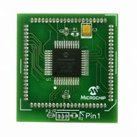
MODULE PLUG-IN PIC18F46J11 PIM
Manufacturer
Microchip Technology
Series
PIC®r
Datasheet
1.MA180023.pdf
(528 pages)
Specifications of MA180023
Accessory Type
Plug-In Module (PIM) - PIC18F46J11
Tool / Board Applications
General Purpose MCU, MPU, DSP, DSC
Mcu Supported Families
PIC18
Supported Devices
Stand-alone Or W/ HPC(DM183022) Or PIC18(DM183032)
Silicon Manufacturer
Microchip
Core Architecture
PIC
Core Sub-architecture
PIC18
Silicon Core Number
PIC18F
Silicon Family Name
PIC18FxxJxx
Lead Free Status / RoHS Status
Lead free / RoHS Compliant
For Use With/related Products
HPC Explorer Board (DM183022) or PIC18 Explorer Board (DM183032)
For Use With
DM183032 - BOARD EXPLORER PICDEM PIC18DM183022 - BOARD DEMO PIC18FXX22 64/80TQFP
Lead Free Status / RoHS Status
Lead free / RoHS Compliant
Available stocks
Company
Part Number
Manufacturer
Quantity
Price
Company:

Part Number:
MA180023
Manufacturer:
Microchip Technology
Quantity:
135


PIC18F46J11 FAMILY
BTFSC
Syntax:
Operands:
Operation:
Status Affected:
Encoding:
Description:
Words:
Cycles:
Example:
DS39932C-page 420
Q Cycle Activity:
If skip:
If skip and followed by 2-word instruction:
Before Instruction
After Instruction
operation
operation
operation
Decode
PC
If FLAG<1>
If FLAG<1>
No
No
No
Q1
Q1
Q1
PC
PC
Bit Test File, Skip if Clear
BTFSC f, b {,a}
0 ≤ f ≤ 255
0 ≤ b ≤ 7
a ∈ [0,1]
skip if (f<b>) = 0
None
If bit ‘b’ in register ‘f’ is ‘0’, then the next
instruction is skipped. If bit ‘b’ is ‘0’,
then the next instruction fetched during
the current instruction execution is dis-
carded and a NOP is executed instead,
making this a two-cycle instruction.
If ‘a’ is ‘0’, the Access Bank is selected.
If ‘a’ is ‘1’, the BSR is used to select the
GPR bank (default).
If ‘a’ is ‘0’ and the extended instruction
set is enabled, this instruction operates
in Indexed Literal Offset Addressing
mode whenever f ≤ 95 (5Fh). See
Section 26.2.3 “Byte-Oriented and
Bit-Oriented Instructions in Indexed
Literal Offset Mode” for details.
1
1(2)
Note: 3 cycles if skip and followed
register ‘f’
HERE
FALSE
TRUE
operation
operation
operation
1011
Read
No
No
No
=
=
=
=
=
Q2
Q2
Q2
by a 2-word instruction.
address (HERE)
0;
address (TRUE)
1;
address (FALSE)
BTFSC
:
:
bbba
operation
operation
operation
Process
Data
No
No
No
Q3
Q3
Q3
FLAG, 1, 0
ffff
operation
operation
operation
operation
No
No
No
No
Q4
Q4
Q4
ffff
BTFSS
Syntax:
Operands:
Operation:
Status Affected:
Encoding:
Description:
Words:
Cycles:
Example:
Q Cycle Activity:
If skip:
If skip and followed by 2-word instruction:
Before Instruction
After Instruction
operation
operation
operation
Decode
PC
If FLAG<1>
If FLAG<1>
No
No
No
Q1
Q1
Q1
PC
PC
Bit Test File, Skip if Set
BTFSS f, b {,a}
0 ≤ f ≤ 255
0 ≤ b < 7
a ∈ [0,1]
skip if (f<b>) = 1
None
If bit ‘b’ in register ‘f’ is ‘1’, then the next
instruction is skipped. If bit ‘b’ is ‘1’,
then the next instruction fetched during
the current instruction execution is dis-
carded and a NOP is executed instead,
making this a two-cycle instruction.
If ‘a’ is ‘0’, the Access Bank is selected.
If ‘a’ is ‘1’, the BSR is used to select the
GPR bank (default).
If ‘a’ is ‘0’ and the extended instruction
set is enabled, this instruction operates
in Indexed Literal Offset Addressing
mode whenever f ≤ 95 (5Fh). See
Section 26.2.3 “Byte-Oriented and
Bit-Oriented Instructions in Indexed
Literal Offset Mode” for details.
1
1(2)
Note:
register ‘f’
HERE
FALSE
TRUE
operation
operation
operation
1010
Read
No
No
No
=
=
=
=
=
Q2
Q2
Q2
© 2009 Microchip Technology Inc.
address (HERE)
0;
address (FALSE)
1;
address (TRUE)
3 cycles if skip and followed
by a 2-word instruction.
BTFSS
:
:
bbba
operation
operation
operation
Process
Data
No
No
No
Q3
Q3
Q3
FLAG, 1, 0
ffff
operation
operation
operation
operation
No
No
No
No
Q4
Q4
Q4
ffff
Related parts for MA180023
Image
Part Number
Description
Manufacturer
Datasheet
Request
R

Part Number:
Description:
Manufacturer:
Microchip Technology Inc.
Datasheet:
Part Number:
Description:
Manufacturer:
Microchip Technology Inc.
Datasheet:
Part Number:
Description:
Manufacturer:
Microchip Technology Inc.
Datasheet:
Part Number:
Description:
Manufacturer:
Microchip Technology Inc.
Datasheet:
Part Number:
Description:
Manufacturer:
Microchip Technology Inc.
Datasheet:
Part Number:
Description:
Manufacturer:
Microchip Technology Inc.
Datasheet:
Part Number:
Description:
Manufacturer:
Microchip Technology Inc.
Datasheet:
Part Number:
Description:
Manufacturer:
Microchip Technology Inc.
Datasheet: