MA180023 Microchip Technology, MA180023 Datasheet - Page 249
MA180023
Manufacturer Part Number
MA180023
Description
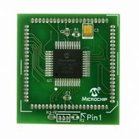
MODULE PLUG-IN PIC18F46J11 PIM
Manufacturer
Microchip Technology
Series
PIC®r
Datasheet
1.MA180023.pdf
(528 pages)
Specifications of MA180023
Accessory Type
Plug-In Module (PIM) - PIC18F46J11
Tool / Board Applications
General Purpose MCU, MPU, DSP, DSC
Mcu Supported Families
PIC18
Supported Devices
Stand-alone Or W/ HPC(DM183022) Or PIC18(DM183032)
Silicon Manufacturer
Microchip
Core Architecture
PIC
Core Sub-architecture
PIC18
Silicon Core Number
PIC18F
Silicon Family Name
PIC18FxxJxx
Lead Free Status / RoHS Status
Lead free / RoHS Compliant
For Use With/related Products
HPC Explorer Board (DM183022) or PIC18 Explorer Board (DM183032)
For Use With
DM183032 - BOARD EXPLORER PICDEM PIC18DM183022 - BOARD DEMO PIC18FXX22 64/80TQFP
Lead Free Status / RoHS Status
Lead free / RoHS Compliant
Available stocks
Company
Part Number
Manufacturer
Quantity
Price
Company:

Part Number:
MA180023
Manufacturer:
Microchip Technology
Quantity:
135


17.5
The Enhanced PWM mode can generate a PWM signal
on up to four different output pins with up to 10 bits of
resolution. It can do this through four different PWM
Output modes:
• Single PWM
• Half-Bridge PWM
• Full-Bridge PWM, Forward mode
• Full-Bridge PWM, Reverse mode
To select an Enhanced PWM mode, the PxM bits of the
CCPxCON register must be set appropriately.
FIGURE 17-5:
© 2009 Microchip Technology Inc.
Note 1: The TRIS register value for each PWM output must be configured appropriately.
Note 1: The 8-bit timer TMR2 register is concatenated with the 2-bit internal Q clock, or 2 bits of the prescaler to
2: Any pin not used by an Enhanced PWM mode is available for alternate pin functions.
PWM (Enhanced Mode)
CCPR1H (Slave)
Duty Cycle Registers
Comparator
2: These pins are remappable.
CCPR1L
PR2
TMR2
Comparator
create the 10-bit time base.
EXAMPLE SIMPLIFIED BLOCK DIAGRAM OF THE ENHANCED PWM MODE
(1)
Clear Timer2,
toggle PWM pin and
latch duty cycle
DC1B<1:0>
R
S
PxM<1:0>
Q
ECCP1DEL
ECCPx/PxA
Controller
Output
PIC18F46J11 FAMILY
2
The PWM outputs are multiplexed with I/O pins and are
designated: PxA, PxB, PxC and PxD. The polarity of the
PWM pins is configurable and is selected by setting the
CCPxM bits in the CCPxCON register appropriately.
Table 17-1 provides the pin assignments for each
Enhanced PWM mode.
Figure 17-5 provides an example of a simplified block
diagram of the Enhanced PWM module.
Note:
PxB
PxC
PxD
4
CCPxM<3:0>
(2)
(2)
(2)
(2)
To
incomplete waveform when the PWM is
first enabled, the ECCP module waits until
the start of a new PWM period before
generating a PWM signal.
TRIS
TRIS
TRIS
TRIS
prevent
the
generation
ECCP1/RPn
RPn
PRn
PRn
DS39932C-page 249
of
an
Related parts for MA180023
Image
Part Number
Description
Manufacturer
Datasheet
Request
R

Part Number:
Description:
Manufacturer:
Microchip Technology Inc.
Datasheet:
Part Number:
Description:
Manufacturer:
Microchip Technology Inc.
Datasheet:
Part Number:
Description:
Manufacturer:
Microchip Technology Inc.
Datasheet:
Part Number:
Description:
Manufacturer:
Microchip Technology Inc.
Datasheet:
Part Number:
Description:
Manufacturer:
Microchip Technology Inc.
Datasheet:
Part Number:
Description:
Manufacturer:
Microchip Technology Inc.
Datasheet:
Part Number:
Description:
Manufacturer:
Microchip Technology Inc.
Datasheet:
Part Number:
Description:
Manufacturer:
Microchip Technology Inc.
Datasheet: