MA180023 Microchip Technology, MA180023 Datasheet - Page 300
MA180023
Manufacturer Part Number
MA180023
Description
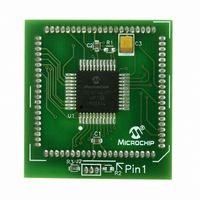
MODULE PLUG-IN PIC18F46J11 PIM
Manufacturer
Microchip Technology
Series
PIC®r
Datasheet
1.MA180023.pdf
(528 pages)
Specifications of MA180023
Accessory Type
Plug-In Module (PIM) - PIC18F46J11
Tool / Board Applications
General Purpose MCU, MPU, DSP, DSC
Mcu Supported Families
PIC18
Supported Devices
Stand-alone Or W/ HPC(DM183022) Or PIC18(DM183032)
Silicon Manufacturer
Microchip
Core Architecture
PIC
Core Sub-architecture
PIC18
Silicon Core Number
PIC18F
Silicon Family Name
PIC18FxxJxx
Lead Free Status / RoHS Status
Lead free / RoHS Compliant
For Use With/related Products
HPC Explorer Board (DM183022) or PIC18 Explorer Board (DM183032)
For Use With
DM183032 - BOARD EXPLORER PICDEM PIC18DM183022 - BOARD DEMO PIC18FXX22 64/80TQFP
Lead Free Status / RoHS Status
Lead free / RoHS Compliant
Available stocks
Company
Part Number
Manufacturer
Quantity
Price
Company:

Part Number:
MA180023
Manufacturer:
Microchip Technology
Quantity:
135


PIC18F46J11 FAMILY
18.5.4
Both 7-Bit and 10-Bit Slave modes implement
automatic clock stretching during a transmit sequence.
The SEN bit (SSPxCON2<0>) allows clock stretching
to be enabled during receives. Setting SEN will cause
the SCLx pin to be held low at the end of each data
receive sequence.
18.5.4.1
In 7-Bit Slave Receive mode, on the falling edge of the
ninth clock at the end of the ACK sequence, if the BF
bit is set, the CKP bit in the SSPxCON1 register is
automatically cleared, forcing the SCLx output to be
held low. The CKP bit being cleared to ‘0’ will assert
the SCLx line low. The CKP bit must be set in the
user’s ISR before reception is allowed to continue. By
holding the SCLx line low, the user has time to service
the ISR and read the contents of the SSPxBUF before
the master device can initiate another receive
sequence. This will prevent buffer overruns from
occurring (see Figure 18-15).
18.5.4.2
In 10-Bit Slave Receive mode, during the address
sequence, clock stretching automatically takes place
but CKP is not cleared. During this time, if the UA bit is
set after the ninth clock, clock stretching is initiated.
The UA bit is set after receiving the upper byte of the
10-bit address and following the receive of the second
byte of the 10-bit address with the R/W bit cleared to
‘0’. The release of the clock line occurs upon updating
SSPxADD. Clock stretching will occur on each data
receive sequence as described in 7-bit mode.
DS39932C-page 300
Note:
Note 1: If the user reads the contents of the
2: The CKP bit can be set in software
CLOCK STRETCHING
If the user polls the UA bit and clears it by
updating the SSPxADD register before the
falling edge of the ninth clock occurs, and
if the user has not cleared the BF bit by
reading the SSPxBUF register before that
time, then the CKP bit will still NOT be
asserted low. Clock stretching on the basis
of the state of the BF bit only occurs during
a
sequence.
SSPxBUF before the falling edge of the
ninth clock, thus clearing the BF bit, the
CKP bit will not be cleared and clock
stretching will not occur.
regardless of the state of the BF bit. The
user should be careful to clear the BF bit
in the ISR before the next receive
sequence in order to prevent an overflow
condition.
Clock Stretching for 7-Bit Slave
Receive Mode (SEN =
Clock Stretching for 10-Bit Slave
Receive Mode (SEN = 1)
data
sequence,
not
1
)
an
address
18.5.4.3
The 7-Bit Slave Transmit mode implements clock
stretching by clearing the CKP bit after the falling edge
of the ninth clock if the BF bit is clear. This occurs
regardless of the state of the SEN bit.
The user’s Interrupt Service Routine (ISR) must set
the CKP bit before transmission is allowed to continue.
By holding the SCLx line low, the user has time to
service the ISR and load the contents of the SSPxBUF
before the master device can initiate another transmit
sequence (see Figure 18-10).
18.5.4.4
In 10-Bit Slave Transmit mode, clock stretching is
controlled during the first two address sequences by
the state of the UA bit, just as it is in 10-Bit Slave
Receive mode. The first two addresses are followed
by a third address sequence, which contains the
high-order bits of the 10-bit address and the R/W bit
set to ‘1’. After the third address sequence is
performed, the UA bit is not set, the module is now
configured in Transmit mode and clock stretching is
controlled by the BF flag as in 7-Bit Slave Transmit
mode (see Figure 18-13).
Note 1: If the user loads the contents of
2: The CKP bit can be set in software
SSPxBUF, setting the BF bit before the
falling edge of the ninth clock, the CKP bit
will not be cleared and clock stretching
will not occur.
regardless of the state of the BF bit.
Clock Stretching for 7-Bit Slave
Transmit Mode
Clock Stretching for 10-Bit Slave
Transmit Mode
© 2009 Microchip Technology Inc.
Related parts for MA180023
Image
Part Number
Description
Manufacturer
Datasheet
Request
R

Part Number:
Description:
Manufacturer:
Microchip Technology Inc.
Datasheet:
Part Number:
Description:
Manufacturer:
Microchip Technology Inc.
Datasheet:
Part Number:
Description:
Manufacturer:
Microchip Technology Inc.
Datasheet:
Part Number:
Description:
Manufacturer:
Microchip Technology Inc.
Datasheet:
Part Number:
Description:
Manufacturer:
Microchip Technology Inc.
Datasheet:
Part Number:
Description:
Manufacturer:
Microchip Technology Inc.
Datasheet:
Part Number:
Description:
Manufacturer:
Microchip Technology Inc.
Datasheet:
Part Number:
Description:
Manufacturer:
Microchip Technology Inc.
Datasheet: