MA180023 Microchip Technology, MA180023 Datasheet - Page 364
MA180023
Manufacturer Part Number
MA180023
Description
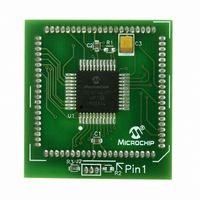
MODULE PLUG-IN PIC18F46J11 PIM
Manufacturer
Microchip Technology
Series
PIC®r
Datasheet
1.MA180023.pdf
(528 pages)
Specifications of MA180023
Accessory Type
Plug-In Module (PIM) - PIC18F46J11
Tool / Board Applications
General Purpose MCU, MPU, DSP, DSC
Mcu Supported Families
PIC18
Supported Devices
Stand-alone Or W/ HPC(DM183022) Or PIC18(DM183032)
Silicon Manufacturer
Microchip
Core Architecture
PIC
Core Sub-architecture
PIC18
Silicon Core Number
PIC18F
Silicon Family Name
PIC18FxxJxx
Lead Free Status / RoHS Status
Lead free / RoHS Compliant
For Use With/related Products
HPC Explorer Board (DM183022) or PIC18 Explorer Board (DM183032)
For Use With
DM183032 - BOARD EXPLORER PICDEM PIC18DM183022 - BOARD DEMO PIC18FXX22 64/80TQFP
Lead Free Status / RoHS Status
Lead free / RoHS Compliant
Available stocks
Company
Part Number
Manufacturer
Quantity
Price
Company:

Part Number:
MA180023
Manufacturer:
Microchip Technology
Quantity:
135


PIC18F46J11 FAMILY
22.1
The comparator voltage reference module is controlled
through the CVRCON register (Register 22-1). The
comparator voltage reference provides two ranges of
output voltage, each with 16 distinct levels. The range
to be used is selected by the CVRR bit (CVRCON<5>).
The primary difference between the ranges is the size
of the steps selected by the CV
(CVR<3:0>), with one range offering finer resolution.
The equations used to calculate the output of the
comparator voltage reference are as follows:
EQUATION 22-1:
REGISTER 22-1:
DS39932C-page 364
When CVRR = 1 and CVRSS = 0:
CV
When CVRR = 0 and CVRSS = 0:
CV
When CVRR = 1 and CVRSS = 1:
CV
When CVRR = 0 and CVRSS = 1:
CV
bit 7
Legend:
R = Readable bit
-n = Value at POR
bit 7
bit 6
bit 5
bit 4
bit 3-0
Note 1:
REF
REF
REF
REF
CVREN
R/W-0
= ((CVR<3:0>)/24) x (CV
= (CV
= ((CVR<3:0>)/24) x (CV
= (CV
Configuring the Comparator
Voltage Reference
RSRC
RSRC
CVROE overrides the TRIS bit setting.
CVREN: Comparator Voltage Reference Enable bit
1 = CV
0 = CV
CVROE: Comparator V
1 = CV
0 = CV
CVRR: Comparator V
1 = 0 to 0.667 CV
0 = 0.25 CV
CVRSS: Comparator V
1 = Comparator reference source, CV
0 = Comparator reference source, CV
CVR<3:0>: Comparator V
When CVRR = 1:
CV
When CVRR = 0:
CV
/4) + ((CVR<3:0>)/32) x (CV
/4) + ((CVR<3:0>)/32) x (CV
CVROE
REF
REF
R/W-0
CALCULATING OUTPUT
OF THE COMPARATOR
VOLTAGE REFERENCE
CVRCON: COMPARATOR VOLTAGE REFERENCE CONTROL REGISTER
(BANKED F53h)
= ((CVR<3:0>)/24) • (CV
= (CV
REF
REF
REF
REF
(1)
circuit powered on
circuit powered down
voltage level is also output on the RA2/AN2/V
voltage is disconnected from the RA2/AN2/V
RSRC
RSRC
RSRC
RSRC
W = Writable bit
‘1’ = Bit is set
)
) + V
R/W-0
CVRR
/4) + ((CVR<3:0>)/32) • (CV
RSRC
to 0.75 CV
REF
REF
REF
REF
REF
, with CV
-
RSRC
RSRC
Selection bits
Range Selection bit
REF
Source Selection bit
Output Enable bit
)
) +V
RSRC
Value Selection bits (0 ≤ (CVR<3:0>) ≤ 15)
REF
CVRSS
RSRC
RSRC
R/W-0
, with CV
-)
)
/24 step size (low range)
RSRC
RSRC
RSRC
U = Unimplemented bit, read as ‘0’
‘0’ = Bit is cleared
= (V
= AV
(1)
RSRC
R/W-0
CVR3
The comparator reference supply voltage can come
from either V
V
voltage source is selected by the CVRSS bit
(CVRCON<4>).
The settling time of the comparator voltage reference
must be considered when changing the CV
output (see Table 28-4 in Section 28.0 “Electrical
Characteristics”).
/32 step size (high range)
REF
DD
REF
)
+) – (V
– AV
- that are multiplexed with RA2 and RA3. The
REF
SS
REF
REF
-/CV
-/CV
DD
-)
R/W-0
CVR2
REF
and V
REF
/C2INB pin
/C2INB pin
SS
© 2009 Microchip Technology Inc.
x = Bit is unknown
, or the external V
R/W-0
CVR1
R/W-0
CVR0
REF
+ and
bit 0
REF
Related parts for MA180023
Image
Part Number
Description
Manufacturer
Datasheet
Request
R

Part Number:
Description:
Manufacturer:
Microchip Technology Inc.
Datasheet:
Part Number:
Description:
Manufacturer:
Microchip Technology Inc.
Datasheet:
Part Number:
Description:
Manufacturer:
Microchip Technology Inc.
Datasheet:
Part Number:
Description:
Manufacturer:
Microchip Technology Inc.
Datasheet:
Part Number:
Description:
Manufacturer:
Microchip Technology Inc.
Datasheet:
Part Number:
Description:
Manufacturer:
Microchip Technology Inc.
Datasheet:
Part Number:
Description:
Manufacturer:
Microchip Technology Inc.
Datasheet:
Part Number:
Description:
Manufacturer:
Microchip Technology Inc.
Datasheet: