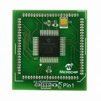
MA180023 Microchip Technology, MA180023 Datasheet - Page 351

MA180023
Manufacturer Part Number
MA180023
Description
MODULE PLUG-IN PIC18F46J11 PIM
Manufacturer
Microchip Technology
Series
PIC®r
Datasheet
1.MA180023.pdf
(528 pages)
Specifications of MA180023
Accessory Type
Plug-In Module (PIM) - PIC18F46J11
Tool / Board Applications
General Purpose MCU, MPU, DSP, DSC
Mcu Supported Families
PIC18
Supported Devices
Stand-alone Or W/ HPC(DM183022) Or PIC18(DM183032)
Silicon Manufacturer
Microchip
Core Architecture
PIC
Core Sub-architecture
PIC18
Silicon Core Number
PIC18F
Silicon Family Name
PIC18FxxJxx
Lead Free Status / RoHS Status
Lead free / RoHS Compliant
For Use With/related Products
HPC Explorer Board (DM183022) or PIC18 Explorer Board (DM183032)
For Use With
DM183032 - BOARD EXPLORER PICDEM PIC18DM183022 - BOARD DEMO PIC18FXX22 64/80TQFP
Lead Free Status / RoHS Status
Lead free / RoHS Compliant
Available stocks
Company
Part Number
Manufacturer
Quantity
Price
Company:
Part Number:
MA180023
Manufacturer:
Microchip Technology
Quantity:
135
- Current page: 351 of 528
- Download datasheet (8Mb)
20.2
The ADCON1 register allows the user to select an
acquisition time that occurs each time the GO/DONE
bit is set.
When the GO/DONE bit is set, sampling is stopped and
a conversion begins. The user is responsible for ensur-
ing the required acquisition time has passed between
selecting the desired input channel and setting the
GO/DONE bit. This occurs when the ACQT<2:0> bits
(ADCON1<5:3>) remain in their Reset state (‘000’) and
is compatible with devices that do not offer
programmable acquisition times.
If desired, the ACQT bits can be set to select a pro-
grammable acquisition time for the A/D module. When
the GO/DONE bit is set, the A/D module continues to
sample the input for the selected acquisition time, then
automatically begins a conversion. Since the acquisi-
tion time is programmed, there may be no need to wait
for an acquisition time between selecting a channel and
setting the GO/DONE bit.
In either case, when the conversion is completed, the
GO/DONE bit is cleared, the ADIF flag is set and the
A/D begins sampling the currently selected channel
again. If an acquisition time is programmed, there is
nothing to indicate if the acquisition time has ended or
if the conversion has begun.
20.3
The A/D conversion time per bit is defined as T
A/D conversion requires 11 T
The source of the A/D conversion clock is software
selectable.
There are seven possible options for T
• 2 T
• 4 T
• 8 T
• 16 T
• 32 T
• 64 T
• Internal RC Oscillator
For correct A/D conversions, the A/D conversion clock
(T
minimum T
more information).
Table 20-1 provides the resultant T
from the device operating frequencies and the A/D
clock source selected.
© 2009 Microchip Technology Inc.
AD
) must be as short as possible but greater than the
OSC
OSC
OSC
OSC
OSC
OSC
Selecting and Configuring
Automatic Acquisition Time
Selecting the A/D Conversion
Clock
AD
(see parameter 130 in Table 28-28 for
AD
per 10-bit conversion.
AD
AD
times derived
:
AD
. The
PIC18F46J11 FAMILY
TABLE 20-1:
20.4
The ANCON0, ANCON1 and TRISA registers control
the operation of the A/D port pins. The port pins needed
as analog inputs must have their corresponding TRIS
bits set (input). If the TRIS bit is cleared (output), the
digital output level (V
The A/D operation is independent of the state of the
CHS<3:0> bits and the TRIS bits.
Note 1:
Note 1: When reading the PORT register, all pins
Operation
16 T
32 T
64 T
2 T
4 T
8 T
AD Clock Source (T
RC
2:
OSC
OSC
OSC
2: Analog levels on any pin defined as a
Configuring Analog Port Pins
OSC
OSC
OSC
(2)
The RC source has a typical T
4 μs.
For device frequencies above 1 MHz, the
device must be in Sleep mode for the
entire conversion or the A/D accuracy may
be out of specification.
configured as analog input channels will
read as cleared (a low level). Pins config-
ured as digital inputs will convert an
analog input. Analog levels on a digitally
configured
converted.
digital input may cause the digital input
buffer to consume current out of the
device’s specification limits.
T
FREQUENCIES
AD
OH
ADCS<2:0>
vs. DEVICE OPERATING
or V
000
100
001
101
010
110
011
input
AD
OL
)
) will be converted.
will
DS39932C-page 351
be
Frequency
22.86 MHz
45.71 MHz
11.43 MHz
Maximum
1.00 MHz
2.86 MHz
5.71 MHz
48.0 MHz
Device
AD
accurately
time of
(1)
Related parts for MA180023
Image
Part Number
Description
Manufacturer
Datasheet
Request
R

Part Number:
Description:
Manufacturer:
Microchip Technology Inc.
Datasheet:

Part Number:
Description:
Manufacturer:
Microchip Technology Inc.
Datasheet:

Part Number:
Description:
Manufacturer:
Microchip Technology Inc.
Datasheet:

Part Number:
Description:
Manufacturer:
Microchip Technology Inc.
Datasheet:

Part Number:
Description:
Manufacturer:
Microchip Technology Inc.
Datasheet:

Part Number:
Description:
Manufacturer:
Microchip Technology Inc.
Datasheet:

Part Number:
Description:
Manufacturer:
Microchip Technology Inc.
Datasheet:

Part Number:
Description:
Manufacturer:
Microchip Technology Inc.
Datasheet:


