MA180023 Microchip Technology, MA180023 Datasheet - Page 274
MA180023
Manufacturer Part Number
MA180023
Description
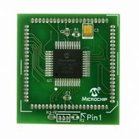
MODULE PLUG-IN PIC18F46J11 PIM
Manufacturer
Microchip Technology
Series
PIC®r
Datasheet
1.MA180023.pdf
(528 pages)
Specifications of MA180023
Accessory Type
Plug-In Module (PIM) - PIC18F46J11
Tool / Board Applications
General Purpose MCU, MPU, DSP, DSC
Mcu Supported Families
PIC18
Supported Devices
Stand-alone Or W/ HPC(DM183022) Or PIC18(DM183032)
Silicon Manufacturer
Microchip
Core Architecture
PIC
Core Sub-architecture
PIC18
Silicon Core Number
PIC18F
Silicon Family Name
PIC18FxxJxx
Lead Free Status / RoHS Status
Lead free / RoHS Compliant
For Use With/related Products
HPC Explorer Board (DM183022) or PIC18 Explorer Board (DM183032)
For Use With
DM183032 - BOARD EXPLORER PICDEM PIC18DM183022 - BOARD DEMO PIC18FXX22 64/80TQFP
Lead Free Status / RoHS Status
Lead free / RoHS Compliant
Available stocks
Company
Part Number
Manufacturer
Quantity
Price
Company:

Part Number:
MA180023
Manufacturer:
Microchip Technology
Quantity:
135


PIC18F46J11 FAMILY
18.3.9
In SPI Master mode, module clocks may be operating
at a different speed than when in full-power mode. In
the case of Sleep mode, all clocks are halted.
In Idle modes, a clock is provided to the peripherals.
That clock can be from the primary clock source, the
secondary clock (Timer1 oscillator) or the INTOSC
source. See Section 2.3 “Clock Sources and
Oscillator Switching” for additional information.
In most cases, the speed that the master clocks SPI
data is not important; however, this should be
evaluated for each system.
If MSSP interrupts are enabled, they can wake the
controller from Sleep mode, or one of the Idle modes,
when the master completes sending data. If an exit
from Sleep or Idle mode is not desired, MSSP
interrupts should be disabled.
If the Sleep mode is selected, all module clocks are
halted and the transmission/reception will remain in
that state until the device wakes. After the device
returns to Run mode, the module will resume
transmitting and receiving data.
In SPI Slave mode, the SPI Transmit/Receive Shift
register operates asynchronously to the device. This
allows the device to be placed in any power-managed
mode
Transmit/Receive Shift register. When all 8 bits have
been received, the MSSP interrupt flag bit will be set,
and if enabled, will wake the device.
18.3.10
A Reset disables the MSSP module and terminates the
current transfer.
DS39932C-page 274
and
OPERATION IN POWER-MANAGED
MODES
EFFECTS OF A RESET
data
to be
shifted into
the
SPI
18.3.11
Table 18-1 provides the compatibility between the
standard SPI modes and the states of the CKP and
CKE control bits.
TABLE 18-1:
There is also an SMP bit, which controls when the data
is sampled.
18.3.12
Because MSSP1 and MSSP2 are independent
modules, they can operate simultaneously at different
data rates. Setting the SSPM<3:0> bits of the
SSPxCON1 register determines the rate for the
corresponding module.
An exception is when both modules use Timer2 as a
time base in Master mode. In this instance, any
changes to the Timer2 module’s operation will affect
both MSSP modules equally. If different bit rates are
required for each module, the user should select one of
the other three time base options for one of the
modules.
Standard SPI Mode
Terminology
0, 0
0, 1
1, 0
1, 1
BUS MODE COMPATIBILITY
SPI CLOCK SPEED AND MODULE
INTERACTIONS
SPI BUS MODES
© 2009 Microchip Technology Inc.
CKP
Control Bits State
0
0
1
1
CKE
1
0
1
0
Related parts for MA180023
Image
Part Number
Description
Manufacturer
Datasheet
Request
R

Part Number:
Description:
Manufacturer:
Microchip Technology Inc.
Datasheet:
Part Number:
Description:
Manufacturer:
Microchip Technology Inc.
Datasheet:
Part Number:
Description:
Manufacturer:
Microchip Technology Inc.
Datasheet:
Part Number:
Description:
Manufacturer:
Microchip Technology Inc.
Datasheet:
Part Number:
Description:
Manufacturer:
Microchip Technology Inc.
Datasheet:
Part Number:
Description:
Manufacturer:
Microchip Technology Inc.
Datasheet:
Part Number:
Description:
Manufacturer:
Microchip Technology Inc.
Datasheet:
Part Number:
Description:
Manufacturer:
Microchip Technology Inc.
Datasheet: