MA180023 Microchip Technology, MA180023 Datasheet - Page 405
MA180023
Manufacturer Part Number
MA180023
Description
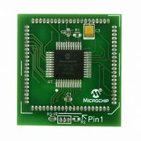
MODULE PLUG-IN PIC18F46J11 PIM
Manufacturer
Microchip Technology
Series
PIC®r
Datasheet
1.MA180023.pdf
(528 pages)
Specifications of MA180023
Accessory Type
Plug-In Module (PIM) - PIC18F46J11
Tool / Board Applications
General Purpose MCU, MPU, DSP, DSC
Mcu Supported Families
PIC18
Supported Devices
Stand-alone Or W/ HPC(DM183022) Or PIC18(DM183032)
Silicon Manufacturer
Microchip
Core Architecture
PIC
Core Sub-architecture
PIC18
Silicon Core Number
PIC18F
Silicon Family Name
PIC18FxxJxx
Lead Free Status / RoHS Status
Lead free / RoHS Compliant
For Use With/related Products
HPC Explorer Board (DM183022) or PIC18 Explorer Board (DM183032)
For Use With
DM183032 - BOARD EXPLORER PICDEM PIC18DM183022 - BOARD DEMO PIC18FXX22 64/80TQFP
Lead Free Status / RoHS Status
Lead free / RoHS Compliant
Available stocks
Company
Part Number
Manufacturer
Quantity
Price
Company:

Part Number:
MA180023
Manufacturer:
Microchip Technology
Quantity:
135


25.5.2
The Fail-Safe Clock Monitor condition is terminated by
either a device Reset or by entering a power-managed
mode. On Reset, the controller starts the primary clock
source specified in Configuration Register 2H (with any
required start-up delays that are required for the oscil-
lator mode, such as OST or PLL timer). The INTRC
oscillator provides the device clock until the primary
clock source becomes ready (similar to a Two-Speed
Start-up). The clock source is then switched to the
primary clock (indicated by the OSTS bit in the
OSCCON register becoming set). The FSCM then
resumes monitoring the peripheral clock.
The primary clock source may never become ready
during start-up. In this case, operation is clocked by the
INTRC oscillator. The OSCCON register will remain in
its Reset state until a power-managed mode is entered.
25.5.3
By entering a power-managed mode, the clock
multiplexer selects the clock source selected by the
OSCCON register. FSCM of the power-managed clock
source resumes in the power-managed mode.
If an oscillator failure occurs during power-managed
operation, the subsequent events depend on whether
or not the oscillator failure interrupt is enabled. If
enabled (OSCFIF = 1), code execution will be clocked
by the INTRC multiplexer. An automatic transition back
to the failed clock source will not occur.
If the interrupt is disabled, subsequent interrupts while
in Idle mode will cause the CPU to begin executing
instructions while being clocked by the INTRC source.
25.5.4
The FSCM is designed to detect oscillator failure at any
point after the device has exited Power-on Reset (POR)
or low-power Sleep mode. When the primary device
clock is either the EC or INTRC modes, monitoring can
begin immediately following these events.
For HS or HSPLL modes, the situation is somewhat
different. Since the oscillator may require a start-up
time considerably longer than the FSCM sample clock
time, a false clock failure may be detected. To prevent
this, the internal oscillator block is automatically config-
ured as the device clock and functions until the primary
clock is stable (the OST and PLL timers have timed
© 2009 Microchip Technology Inc.
EXITING FAIL-SAFE OPERATION
POR OR WAKE-UP FROM SLEEP
FSCM INTERRUPTS IN
POWER-MANAGED MODES
PIC18F46J11 FAMILY
out). This is identical to Two-Speed Start-up mode.
Once the primary clock is stable, the INTRC returns to
its role as the FSCM source.
As noted in Section 25.4.1 “Special Considerations
for Using Two-Speed Start-up”, it is also possible to
select another clock configuration and enter an alternate
power-managed mode while waiting for the primary
clock to become stable. When the new power-managed
mode is selected, the primary clock is disabled.
25.6
For all devices in the PIC18F46J11 family of devices,
the on-chip program memory space is treated as a
single block. Code protection for this block is controlled
by one Configuration bit, CP0. This bit inhibits external
reads and writes to the program memory space. It has
no direct effect in normal execution mode.
25.6.1
The Configuration registers are protected against
untoward changes or reads in two ways. The primary
protection is the write-once feature of the Configuration
bits, which prevents reconfiguration once the bit has
been programmed during a power cycle. To safeguard
against
changes resulting from individual cell level disruptions
(such as ESD events) will cause a parity error and
trigger a device Reset. This is seen by the user as a
Configuration Mismatch (CM) Reset.
The data for the Configuration registers is derived from
the FCW in program memory. When the CP0 bit is set,
the source data for device configuration is also
protected as a consequence.
Note:
Program Verification and Code
Protection
unpredictable
The same logic that prevents false
oscillator failure interrupts on POR, or
wake-up from Sleep, will also prevent the
detection of the oscillator’s failure to start
at all following these events. This can be
avoided by monitoring the OSTS bit and
using a timing routine to determine if the
oscillator is taking too long to start. Even
so, no oscillator failure interrupt will be
flagged.
CONFIGURATION REGISTER
PROTECTION
events,
DS39932C-page 405
Configuration
bit
Related parts for MA180023
Image
Part Number
Description
Manufacturer
Datasheet
Request
R

Part Number:
Description:
Manufacturer:
Microchip Technology Inc.
Datasheet:
Part Number:
Description:
Manufacturer:
Microchip Technology Inc.
Datasheet:
Part Number:
Description:
Manufacturer:
Microchip Technology Inc.
Datasheet:
Part Number:
Description:
Manufacturer:
Microchip Technology Inc.
Datasheet:
Part Number:
Description:
Manufacturer:
Microchip Technology Inc.
Datasheet:
Part Number:
Description:
Manufacturer:
Microchip Technology Inc.
Datasheet:
Part Number:
Description:
Manufacturer:
Microchip Technology Inc.
Datasheet:
Part Number:
Description:
Manufacturer:
Microchip Technology Inc.
Datasheet: