MA180023 Microchip Technology, MA180023 Datasheet - Page 181
MA180023
Manufacturer Part Number
MA180023
Description
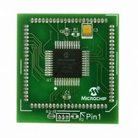
MODULE PLUG-IN PIC18F46J11 PIM
Manufacturer
Microchip Technology
Series
PIC®r
Datasheet
1.MA180023.pdf
(528 pages)
Specifications of MA180023
Accessory Type
Plug-In Module (PIM) - PIC18F46J11
Tool / Board Applications
General Purpose MCU, MPU, DSP, DSC
Mcu Supported Families
PIC18
Supported Devices
Stand-alone Or W/ HPC(DM183022) Or PIC18(DM183032)
Silicon Manufacturer
Microchip
Core Architecture
PIC
Core Sub-architecture
PIC18
Silicon Core Number
PIC18F
Silicon Family Name
PIC18FxxJxx
Lead Free Status / RoHS Status
Lead free / RoHS Compliant
For Use With/related Products
HPC Explorer Board (DM183022) or PIC18 Explorer Board (DM183032)
For Use With
DM183032 - BOARD EXPLORER PICDEM PIC18DM183022 - BOARD DEMO PIC18FXX22 64/80TQFP
Lead Free Status / RoHS Status
Lead free / RoHS Compliant
Available stocks
Company
Part Number
Manufacturer
Quantity
Price
Company:

Part Number:
MA180023
Manufacturer:
Microchip Technology
Quantity:
135


10.3.5
Up to two chip select lines, PMCS1 and PMCS2, are
available for the Master modes of the PMP. The two
chip select lines are multiplexed with the Most Signifi-
cant bit (MSb) of the address bus (PMADDRH<6>).
When a pin is configured as a chip select, it is not
included in any address auto-increment/decrement.
The function of the chip select signals is configured
using the chip select function bits (PMCONL<7:6>).
10.3.6
While the module is operating in one of the Master
modes, the INCMx bits (PMMODEH<4:3>) control the
behavior of the address value. The address can be
made to automatically increment or decrement after
each read and write operation. The address increments
once each operation is completed and the BUSY bit
goes to ‘0’. If the chip select signals are disabled and
configured as address bits, the bits will participate in
the increment and decrement operations; otherwise,
the CS1 bit values will be unaffected.
10.3.7
In Master mode, the user has control over the duration
of the read, write and address cycles by configuring the
module Wait states. Three portions of the cycle, the
beginning, middle and end, are configured using the
corresponding WAITBx, WAITMx and WAITEx bits in
the PMMODEL register.
The WAITBx bits (PMMODEL<7:6>) set the number of
Wait cycles for the data setup prior to the
PMRD/PMWT strobe in Mode 10, or prior to the
PMENB strobe in Mode 11. The WAITMx bits
(PMMODEL<5:2>) set the number of Wait cycles for
the PMRD/PMWT strobe in Mode 10, or for the PMENB
strobe in Mode 11. When this Wait state setting is ‘0’,
then WAITB and WAITE have no effect. The WAITE
bits (PMMODEL<1:0>) define the number of Wait
cycles for the data hold time after the PMRD/PMWT
strobe in Mode 10, or after the PMENB strobe in
Mode 11.
10.3.8
To perform a read on the PMP, the user reads the
PMDIN1L register. This causes the PMP to output the
desired values on the chip select lines and the address
bus. Then the read line (PMRD) is strobed. The read
data is placed into the PMDIN1L register.
If the 16-bit mode is enabled (MODE16 = 1), the read
of the low byte of the PMDIN1L register will initiate two
bus reads. The first read data byte is placed into the
PMDIN1L register, and the second read data is placed
into the PMDIN1H.
© 2009 Microchip Technology Inc.
WAIT STATES
CHIP SELECT FEATURES
AUTO-INCREMENT/DECREMENT
READ OPERATION
PIC18F46J11 FAMILY
Note that the read data obtained from the PMDIN1L
register is actually the read value from the previous
read operation. Hence, the first user read will be a
dummy read to initiate the first bus read and fill the read
register. Also, the requested read value will not be
ready until after the BUSY bit is observed low. Thus, in
a back-to-back read operation, the data read from the
register will be the same for both reads. The next read
of the register will yield the new value.
10.3.9
To perform a write onto the parallel bus, the user writes
to the PMDIN1L register. This causes the module to
first output the desired values on the chip select lines
and the address bus. The write data from the PMDIN1L
register is placed onto the PMD<7:0> data bus. Then
the write line (PMWR) is strobed. If the 16-bit mode is
enabled (MODE16 = 1), the write to the PMDIN1L
register will initiate two bus writes. First write will
consist of the data contained in PMDIN1L and the
second write will contain the PMDIN1H.
10.3.10
10.3.10.1
In addition to the PMP interrupt, a BUSY bit is provided
to indicate the status of the module. This bit is used
only in Master mode. While any read or write operation
is in progress, the BUSY bit is set for all but the very last
CPU cycle of the operation. In effect, if a single-cycle
read or write operation is requested, the BUSY bit will
never be active. This allows back-to-back transfers.
While the bit is set, any request by the user to initiate a
new operation will be ignored (i.e., writing or reading
the lower byte of the PMDIN1L register will neither
initiate a read nor a write).
10.3.10.2
When the PMP module interrupt is enabled for Master
mode, the module will interrupt on every completed
read or write cycle; otherwise, the BUSY bit is available
to query the status of the module.
WRITE OPERATION
PARALLEL MASTER PORT STATUS
The BUSY Bit
Interrupts
DS39932C-page 181
Related parts for MA180023
Image
Part Number
Description
Manufacturer
Datasheet
Request
R

Part Number:
Description:
Manufacturer:
Microchip Technology Inc.
Datasheet:
Part Number:
Description:
Manufacturer:
Microchip Technology Inc.
Datasheet:
Part Number:
Description:
Manufacturer:
Microchip Technology Inc.
Datasheet:
Part Number:
Description:
Manufacturer:
Microchip Technology Inc.
Datasheet:
Part Number:
Description:
Manufacturer:
Microchip Technology Inc.
Datasheet:
Part Number:
Description:
Manufacturer:
Microchip Technology Inc.
Datasheet:
Part Number:
Description:
Manufacturer:
Microchip Technology Inc.
Datasheet:
Part Number:
Description:
Manufacturer:
Microchip Technology Inc.
Datasheet: