MA180023 Microchip Technology, MA180023 Datasheet - Page 142
MA180023
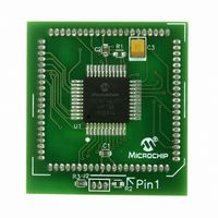
Manufacturer Part Number
MA180023
Description
MODULE PLUG-IN PIC18F46J11 PIM
Manufacturer
Microchip Technology
Series
PIC®r
Datasheet
1.MA180023.pdf
(528 pages)
Specifications of MA180023
Accessory Type
Plug-In Module (PIM) - PIC18F46J11
Tool / Board Applications
General Purpose MCU, MPU, DSP, DSC
Mcu Supported Families
PIC18
Supported Devices
Stand-alone Or W/ HPC(DM183022) Or PIC18(DM183032)
Silicon Manufacturer
Microchip
Core Architecture
PIC
Core Sub-architecture
PIC18
Silicon Core Number
PIC18F
Silicon Family Name
PIC18FxxJxx
Lead Free Status / RoHS Status
Lead free / RoHS Compliant
For Use With/related Products
HPC Explorer Board (DM183022) or PIC18 Explorer Board (DM183032)
For Use With
DM183032 - BOARD EXPLORER PICDEM PIC18DM183022 - BOARD DEMO PIC18FXX22 64/80TQFP
Lead Free Status / RoHS Status
Lead free / RoHS Compliant
Available stocks
Company
Part Number
Manufacturer
Quantity
Price
Company:

Part Number:
MA180023
Manufacturer:
Microchip Technology
Quantity:
135


PIC18F46J11 FAMILY
9.6
Depending on the particular PIC18F46J11 family
device selected, PORTE is implemented in two
different ways.
For 44-pin devices, PORTE is a 3-bit wide port. Three
pins (RE0/AN5/PMRD, RE1/AN6/PMWR and RE2/
AN7/PMCS) are individually configurable as inputs or
outputs. These pins have Schmitt Trigger input buffers.
When selected as analog inputs, these pins will read as
‘0’s.
The corresponding Data Direction register is TRISE.
Setting a TRISE bit (= 1) will make the corresponding
PORTE pin an input (i.e., put the corresponding output
driver in a high-impedance mode). Clearing a TRISE bit
(= 0) will make the corresponding PORTE pin an output
(i.e., put the contents of the output latch on the selected
pin).
TRISE controls the direction of the RE pins, even when
they are being used as analog inputs. The user must
make sure to keep the pins configured as inputs when
using them as analog inputs.
DS39932C-page 142
Note:
Note:
PORTE, TRISE and LATE
Registers
PORTE is available only in 44-pin devices.
On a POR, RE<2:0> are configured as
analog inputs.
The Data Latch register (LATE) is also memory
mapped. Read-modify-write operations on the LATE
register read and write the latched output value for
PORTE.
EXAMPLE 9-6:
Each of the PORTE pins has a weak internal pull-up. A
single control bit can turn on all the pull-ups. This is per-
formed by setting bit, REPU (PORTE<6>). The weak
pull-up is automatically turned off when the port pin is
configured as an output. The pull-ups are disabled on a
POR.
Note that the pull-ups can be used for any set of
features, similar to the pull-ups found on PORTB.
CLRF
CLRF
MOVLW
MOVWF
MOVLW
MOVWF
PORTE
LATE
0Ah
ADCON1
03h
TRISE
; Initialize PORTE by
; clearing output
; data latches
; Alternate method
; to clear output
; data latches
; Configure A/D
; for digital inputs
; Value used to
; initialize data
; direction
; Set RE<0> as inputs
; RE<1> as outputs
; RE<2> as inputs
INITIALIZING PORTE
© 2009 Microchip Technology Inc.
Related parts for MA180023
Image
Part Number
Description
Manufacturer
Datasheet
Request
R

Part Number:
Description:
Manufacturer:
Microchip Technology Inc.
Datasheet:
Part Number:
Description:
Manufacturer:
Microchip Technology Inc.
Datasheet:
Part Number:
Description:
Manufacturer:
Microchip Technology Inc.
Datasheet:
Part Number:
Description:
Manufacturer:
Microchip Technology Inc.
Datasheet:
Part Number:
Description:
Manufacturer:
Microchip Technology Inc.
Datasheet:
Part Number:
Description:
Manufacturer:
Microchip Technology Inc.
Datasheet:
Part Number:
Description:
Manufacturer:
Microchip Technology Inc.
Datasheet:
Part Number:
Description:
Manufacturer:
Microchip Technology Inc.
Datasheet: