MA180023 Microchip Technology, MA180023 Datasheet - Page 147
MA180023
Manufacturer Part Number
MA180023
Description
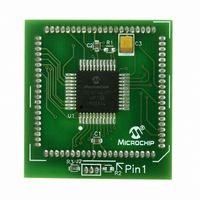
MODULE PLUG-IN PIC18F46J11 PIM
Manufacturer
Microchip Technology
Series
PIC®r
Datasheet
1.MA180023.pdf
(528 pages)
Specifications of MA180023
Accessory Type
Plug-In Module (PIM) - PIC18F46J11
Tool / Board Applications
General Purpose MCU, MPU, DSP, DSC
Mcu Supported Families
PIC18
Supported Devices
Stand-alone Or W/ HPC(DM183022) Or PIC18(DM183032)
Silicon Manufacturer
Microchip
Core Architecture
PIC
Core Sub-architecture
PIC18
Silicon Core Number
PIC18F
Silicon Family Name
PIC18FxxJxx
Lead Free Status / RoHS Status
Lead free / RoHS Compliant
For Use With/related Products
HPC Explorer Board (DM183022) or PIC18 Explorer Board (DM183032)
For Use With
DM183032 - BOARD EXPLORER PICDEM PIC18DM183022 - BOARD DEMO PIC18FXX22 64/80TQFP
Lead Free Status / RoHS Status
Lead free / RoHS Compliant
Available stocks
Company
Part Number
Manufacturer
Quantity
Price
Company:

Part Number:
MA180023
Manufacturer:
Microchip Technology
Quantity:
135


9.7.3.3
The control schema of the PPS is extremely flexible.
Other than systematic blocks that prevent signal con-
tention caused by two physical pins being configured
as the same functional input or two functional outputs
configured as the same pin, there are no hardware
enforced lock outs. The flexibility extends to the point of
allowing a single input to drive multiple peripherals or a
single functional output to drive multiple output pins.
9.7.4
Because peripheral remapping can be changed during
run time, some restrictions on peripheral remapping
are needed to prevent accidental configuration
changes. PIC18F devices include three features to
prevent alterations to the peripheral map:
• Control register lock sequence
• Continuous state monitoring
• Configuration bit remapping lock
9.7.4.1
Under normal operation, writes to the RPINRx and
RPORx registers are not allowed. Attempted writes will
appear to execute normally, but the contents of the
registers will remain unchanged. To change these reg-
isters, they must be unlocked in hardware. The register
lock is controlled by the IOLOCK bit (PPSCON<0>).
Setting IOLOCK prevents writes to the control
registers; clearing IOLOCK allows writes.
To set or clear IOLOCK, a specific command sequence
must be executed:
1.
2.
3.
IOLOCK remains in one state until changed. This
allows all of the PPS registers to be configured with a
single unlock sequence followed by an update to all
control registers, then locked with a second lock
sequence.
9.7.4.2
In addition to being protected from direct writes, the
contents of the RPINRx and RPORx registers are
constantly monitored in hardware by shadow registers.
If an unexpected change in any of the registers occurs
(such as cell disturbances caused by ESD or other
external events), a Configuration Mismatch Reset will
be triggered.
© 2009 Microchip Technology Inc.
Write 55h to EECON2<7:0>.
Write AAh to EECON2<7:0>.
Clear (or set) IOLOCK as a single operation.
CONTROLLING CONFIGURATION
CHANGES
Mapping Limitations
Control Register Lock
Continuous State Monitoring
PIC18F46J11 FAMILY
9.7.4.3
As an additional level of safety, the device can be con-
figured to prevent more than one write session to the
RPINRx and RPORx registers. The IOL1WAY
(CONFIG3H<0>) Configuration bit blocks the IOLOCK
bit from being cleared after it has been set once. If
IOLOCK remains set, the register unlock procedure will
not execute and the PPS control registers cannot be
written to. The only way to clear the bit and re-enable
peripheral remapping is to perform a device Reset.
In the default (unprogrammed) state, IOL1WAY is set,
restricting users to one write session. Programming
IOL1WAY allows users unlimited access (with the
proper use of the unlock sequence) to the PPS
registers.
9.7.5
The ability to control peripheral pin selection introduces
several considerations into application design that
could be overlooked. This is particularly true for several
common peripherals that are available only as
remappable peripherals.
The main consideration is that the PPS is not available
on default pins in the device’s default (Reset) state.
Since all RPINRx registers reset to ‘11111’ and all
RPORx registers reset to ‘00000’, all PPS inputs are
tied to RP31 and all PPS outputs are disconnected.
This situation requires the user to initialize the device
with the proper peripheral configuration before any
other application code is executed. Since the IOLOCK
bit resets in the unlocked state, it is not necessary to
execute the unlock sequence after the device has
come out of Reset.
For application safety, however, it is best to set
IOLOCK and lock the configuration after writing to the
control registers.
Because the unlock sequence is timing critical, it must
be executed as an assembly language routine. If the
bulk of the application is written in C or another high-
level language, the unlock sequence should be
performed by writing in-line assembly.
Note:
CONSIDERATIONS FOR
PERIPHERAL PIN SELECTION
In tying PPS inputs to RP31, RP31 does
not have to exist on a device for the
registers to be reset to it.
Configuration Bit Pin Select Lock
DS39932C-page 147
Related parts for MA180023
Image
Part Number
Description
Manufacturer
Datasheet
Request
R

Part Number:
Description:
Manufacturer:
Microchip Technology Inc.
Datasheet:
Part Number:
Description:
Manufacturer:
Microchip Technology Inc.
Datasheet:
Part Number:
Description:
Manufacturer:
Microchip Technology Inc.
Datasheet:
Part Number:
Description:
Manufacturer:
Microchip Technology Inc.
Datasheet:
Part Number:
Description:
Manufacturer:
Microchip Technology Inc.
Datasheet:
Part Number:
Description:
Manufacturer:
Microchip Technology Inc.
Datasheet:
Part Number:
Description:
Manufacturer:
Microchip Technology Inc.
Datasheet:
Part Number:
Description:
Manufacturer:
Microchip Technology Inc.
Datasheet: