MA180023 Microchip Technology, MA180023 Datasheet - Page 347
MA180023
Manufacturer Part Number
MA180023
Description
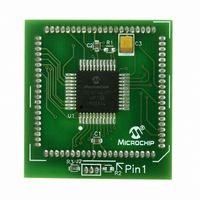
MODULE PLUG-IN PIC18F46J11 PIM
Manufacturer
Microchip Technology
Series
PIC®r
Datasheet
1.MA180023.pdf
(528 pages)
Specifications of MA180023
Accessory Type
Plug-In Module (PIM) - PIC18F46J11
Tool / Board Applications
General Purpose MCU, MPU, DSP, DSC
Mcu Supported Families
PIC18
Supported Devices
Stand-alone Or W/ HPC(DM183022) Or PIC18(DM183032)
Silicon Manufacturer
Microchip
Core Architecture
PIC
Core Sub-architecture
PIC18
Silicon Core Number
PIC18F
Silicon Family Name
PIC18FxxJxx
Lead Free Status / RoHS Status
Lead free / RoHS Compliant
For Use With/related Products
HPC Explorer Board (DM183022) or PIC18 Explorer Board (DM183032)
For Use With
DM183032 - BOARD EXPLORER PICDEM PIC18DM183022 - BOARD DEMO PIC18FXX22 64/80TQFP
Lead Free Status / RoHS Status
Lead free / RoHS Compliant
Available stocks
Company
Part Number
Manufacturer
Quantity
Price
Company:

Part Number:
MA180023
Manufacturer:
Microchip Technology
Quantity:
135


The ANCON0 and ANCON1 registers are used to
configure the operation of the I/O pin associated with
each analog channel. Setting any one of the PCFG bits
configures the corresponding pin to operate as a digital
only I/O. Clearing a bit configures the pin to operate as
an analog input for either the A/D Converter or the
comparator module; all digital peripherals are disabled
and digital inputs read as ‘0’. As a rule, I/O pins that are
multiplexed with analog inputs default to analog
operation on device Resets.
In order to correctly perform A/D conversions on the V
band gap reference (ADCON0<5:2> = 1111), the refer-
ence circuit must be powered on first. The VBGEN bit in
the ANCON1 register allows the firmware to manually
REGISTER 20-3:
REGISTER 20-4:
© 2009 Microchip Technology Inc.
bit 7
Legend:
R = Readable bit
-n = Value at POR
bit 7-0
Note 1:
bit 7
Legend:
R = Readable bit
-n = Value at POR
bit 7
bit 6
bit 5
bit 4-0
PCFG7
VBGEN
R/W-0
R/W-0
(1)
These bits are not implemented on 28-pin devices.
PCFG<7:0>: Analog Port Configuration bits (AN<7:0>)
1 = Pin configured as a digital port
0 = Pin configured as an analog channel – digital input disabled and reads ‘0’
VBGEN: 1.2V Band Gap Reference Enable bit
1 = 1.2V band gap reference is powered on
0 = 1.2V band gap reference is turned off to save power (if no other modules are requesting it)
Reserved: Always maintain as ‘0’ for lowest power consumption
Unimplemented: Read as ‘0’
PCFG<12:8>: Analog Port Configuration bits (AN<12:8>)
1 = Pin configured as a digital port
0 = Pin configured as an analog channel – digital input disabled and reads ‘0’
PCFG6
R/W-0
—
r
ANCON0: A/D PORT CONFIGURATION REGISTER 2 (BANKED F48h)
ANCON1: A/D PORT CONFIGURATION REGISTER 1 (BANKED F49h)
(1)
W = Writable bit
r = Reserved
W = Writable bit
‘1’ = Bit is set
‘1’ = Bit is set
PCFG5
R/W-0
U-0
—
(1)
PCFG12
PCFG4
R/W-0
R/W-0
BG
U = Unimplemented bit, read as ‘0’
‘0’ = Bit is cleared
U = Unimplemented bit, read as ‘0’
‘0’ = Bit is cleared
PIC18F46J11 FAMILY
PCFG11
PCFG3
R/W-0
R/W-0
request that the band gap reference circuit should be
enabled. For best accuracy, firmware should allow a
settling time of at least 10 ms prior to performing the first
acquisition on this channel after enabling the band gap
reference.
The reference circuit may already have been turned on
if some other hardware module (such as the on-chip
voltage regulator, comparators or HLVD) has already
requested it. In this case, the initial turn-on settling time
may have already elapsed and firmware does not need
to wait as long before measuring V
sition is complete, firmware may clear the VBGEN bit,
which will save a small amount of power if no other
modules are still requesting the V
PCFG10
PCFG2
R/W-0
R/W-0
x = Bit is unknown
x = Bit is unknown
PCFG1
PCFG9
R/W-0
R/W-0
BG
BG
DS39932C-page 347
reference.
. Once the acqui-
PCFG0
PCFG8
R/W-0
R/W-0
bit 0
bit 0
Related parts for MA180023
Image
Part Number
Description
Manufacturer
Datasheet
Request
R

Part Number:
Description:
Manufacturer:
Microchip Technology Inc.
Datasheet:
Part Number:
Description:
Manufacturer:
Microchip Technology Inc.
Datasheet:
Part Number:
Description:
Manufacturer:
Microchip Technology Inc.
Datasheet:
Part Number:
Description:
Manufacturer:
Microchip Technology Inc.
Datasheet:
Part Number:
Description:
Manufacturer:
Microchip Technology Inc.
Datasheet:
Part Number:
Description:
Manufacturer:
Microchip Technology Inc.
Datasheet:
Part Number:
Description:
Manufacturer:
Microchip Technology Inc.
Datasheet:
Part Number:
Description:
Manufacturer:
Microchip Technology Inc.
Datasheet: