MA180023 Microchip Technology, MA180023 Datasheet - Page 497
MA180023
Manufacturer Part Number
MA180023
Description
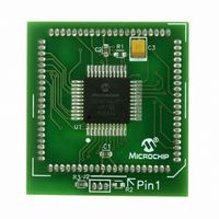
MODULE PLUG-IN PIC18F46J11 PIM
Manufacturer
Microchip Technology
Series
PIC®r
Datasheet
1.MA180023.pdf
(528 pages)
Specifications of MA180023
Accessory Type
Plug-In Module (PIM) - PIC18F46J11
Tool / Board Applications
General Purpose MCU, MPU, DSP, DSC
Mcu Supported Families
PIC18
Supported Devices
Stand-alone Or W/ HPC(DM183022) Or PIC18(DM183032)
Silicon Manufacturer
Microchip
Core Architecture
PIC
Core Sub-architecture
PIC18
Silicon Core Number
PIC18F
Silicon Family Name
PIC18FxxJxx
Lead Free Status / RoHS Status
Lead free / RoHS Compliant
For Use With/related Products
HPC Explorer Board (DM183022) or PIC18 Explorer Board (DM183032)
For Use With
DM183032 - BOARD EXPLORER PICDEM PIC18DM183022 - BOARD DEMO PIC18FXX22 64/80TQFP
Lead Free Status / RoHS Status
Lead free / RoHS Compliant
Available stocks
Company
Part Number
Manufacturer
Quantity
Price
Company:

Part Number:
MA180023
Manufacturer:
Microchip Technology
Quantity:
135


TABLE 28-27: A/D CONVERTER CHARACTERISTICS: PIC18F46J11 FAMILY (INDUSTRIAL)
FIGURE 28-22:
© 2009 Microchip Technology Inc.
Param
A01
A03
A04
A06
A07
A10
A20
A21
A22
A25
A30
A50
Note 1:
No.
Note 1: If the A/D clock source is selected as RC, a time of T
A/D DATA
SAMPLE
2:
A/D CLK
ADRES
Symbol
N
E
E
E
E
ΔV
V
V
V
Z
I
BSF ADCON0, GO
REF
ADIF
REFH
REFL
AIN
AIN
R
IL
DL
OFF
GN
2: This is a minimal RC delay (typically 100 ns), which also disconnects the holding capacitor from the analog input.
GO
REF
The A/D conversion result never decreases with an increase in the input voltage and has no missing codes.
V
V
Q4
REFH
REFL
This allows the SLEEP instruction to be executed.
Resolution
Integral Linearity Error
Differential Linearity Error
Offset Error
Gain Error
Monotonicity
Reference Voltage Range
(V
Reference Voltage High
Reference Voltage Low
Analog Input Voltage
Recommended Impedance of
Analog Voltage Source
V
current is from RA2/AN2/V
132
current is from RA3/AN3/V
REF
REFH
A/D CONVERSION TIMING
Input Current
– V
Characteristic
REFL
(Note 2)
)
9
(2)
8
REF
REF
OLD_DATA
-/CV
7
+/C1INB pin or V
V
REF
SS
. . .
SAMPLING STOPPED
V
V
Min
2.0
REFL
/C2INB pin or V
—
—
—
—
—
—
—
—
– 0.3V
3
SS
. . .
CY
131
130
PIC18F46J11 FAMILY
Guaranteed
is added before the A/D clock starts.
DD
Typ
—
—
—
—
—
—
—
—
—
—
—
—
—
, whichever is selected as the V
2
SS
(1)
, whichever is selected as the V
V
1
DD
V
V
<±3.5
Max
<±1
<±1
<±3
150
REFH
REFH
2.5
10
—
—
– 3.0V
5
0
Units
LSb ΔV
LSb ΔV
LSb ΔV
LSb ΔV
kΩ
μA
μA
bit
—
V
V
V
V
V
ΔV
V
V
V
During V
During A/D conversion
cycle.
NEW_DATA
DONE
SS
DD
DD
REF
REF
REF
REF
REF
DS39932C-page 497
≤ V
< 3.0V
≥ 3.0V
REFH
Conditions
T
CY
≥ 3.0V
≥ 3.0V
≥ 3.0V
≥ 3.0V
≥ 3.0V
AIN
AIN
(Note 1)
source.
REFL
≤ V
acquisition.
REF
source.
Related parts for MA180023
Image
Part Number
Description
Manufacturer
Datasheet
Request
R

Part Number:
Description:
Manufacturer:
Microchip Technology Inc.
Datasheet:
Part Number:
Description:
Manufacturer:
Microchip Technology Inc.
Datasheet:
Part Number:
Description:
Manufacturer:
Microchip Technology Inc.
Datasheet:
Part Number:
Description:
Manufacturer:
Microchip Technology Inc.
Datasheet:
Part Number:
Description:
Manufacturer:
Microchip Technology Inc.
Datasheet:
Part Number:
Description:
Manufacturer:
Microchip Technology Inc.
Datasheet:
Part Number:
Description:
Manufacturer:
Microchip Technology Inc.
Datasheet:
Part Number:
Description:
Manufacturer:
Microchip Technology Inc.
Datasheet: