MA180023 Microchip Technology, MA180023 Datasheet - Page 289
MA180023
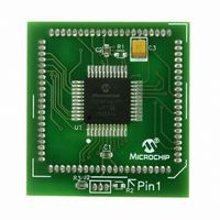
Manufacturer Part Number
MA180023
Description
MODULE PLUG-IN PIC18F46J11 PIM
Manufacturer
Microchip Technology
Series
PIC®r
Datasheet
1.MA180023.pdf
(528 pages)
Specifications of MA180023
Accessory Type
Plug-In Module (PIM) - PIC18F46J11
Tool / Board Applications
General Purpose MCU, MPU, DSP, DSC
Mcu Supported Families
PIC18
Supported Devices
Stand-alone Or W/ HPC(DM183022) Or PIC18(DM183032)
Silicon Manufacturer
Microchip
Core Architecture
PIC
Core Sub-architecture
PIC18
Silicon Core Number
PIC18F
Silicon Family Name
PIC18FxxJxx
Lead Free Status / RoHS Status
Lead free / RoHS Compliant
For Use With/related Products
HPC Explorer Board (DM183022) or PIC18 Explorer Board (DM183032)
For Use With
DM183032 - BOARD EXPLORER PICDEM PIC18DM183022 - BOARD DEMO PIC18FXX22 64/80TQFP
Lead Free Status / RoHS Status
Lead free / RoHS Compliant
Available stocks
Company
Part Number
Manufacturer
Quantity
Price
Company:

Part Number:
MA180023
Manufacturer:
Microchip Technology
Quantity:
135


REGISTER 18-8:
REGISTER 18-9:
© 2009 Microchip Technology Inc.
bit 7
Legend:
R = Readable bit
-n = Value at POR
bit 7
bit 6
bit 5-2
bit 1
bit 0
Note 1:
bit 7
Legend:
R = Readable bit
-n = Value at POR
bit 7-0
Note 1:
GCEN
R/W-0
R/W-1
MSK7
2:
2:
If the I
(or writes to the SSPxBUF are disabled).
This bit is unimplemented in I
This register shares the same SFR address as SSPxADD and is only addressable in select MSSP
operating modes. See Section 18.5.3.4 “7-Bit Address Masking Mode” for more details.
MSK0 is not used as a mask bit in 7-bit addressing.
GCEN: General Call Enable bit (Slave mode only)
1 = Enables interrupt when a general call address (0000h) is received in the SSPxSR
0 = General call address disabled
ACKSTAT: Acknowledge Status bit
Unused in Slave mode.
ADMSK<5:2>: Slave Address Mask Select bits (5-Bit Address Masking)
1 = Masking of corresponding bits of SSPxADD enabled
0 = Masking of corresponding bits of SSPxADD disabled
ADMSK1: Slave Address Least Significant bit(s) Mask Select bit
In 7-Bit Addressing mode:
1 = Masking of SSPxADD<1> only enabled
0 = Masking of SSPxADD<1> only disabled
In 10-Bit Addressing mode:
1 = Masking of SSPxADD<1:0> enabled
0 = Masking of SSPxADD<1:0> disabled
SEN: Start Condition Enable/Stretch Enable bit
1 = Clock stretching is enabled for both slave transmit and slave receive (stretch enabled)
0 = Clock stretching is disabled
MSK<7:0>: Slave Address Mask Select bits
1 = Masking of corresponding bit of SSPxADD enabled
0 = Masking of corresponding bit of SSPxADD disabled
ACKSTAT
2
R/W-0
C module is active, these bits may not be set (no spooling) and the SSPxBUF may not be written
R/W-1
MSK6
SSPxCON2: MSSPx CONTROL REGISTER 2 – I
(ACCESS FC5h/F71h)
SSPxMSK: I
(ACCESS FC8h/F74h)
(2)
W = Writable bit
‘1’ = Bit is set
W = Writable bit
‘1’ = Bit is set
ADMSK5
R/W-0
R/W-1
MSK5
2
C™ SLAVE ADDRESS MASK REGISTER – 7-BIT MASKING MODE
2
C Slave mode.
ADMSK4
R/W-0
(1)
R/W-1
MSK4
(2)
U = Unimplemented bit, read as ‘0’
‘0’ = Bit is cleared
U = Unimplemented bit, read as ‘0’
‘0’ = Bit is cleared
ADMSK3
PIC18F46J11 FAMILY
(1)
R/W-0
R/W-1
MSK3
ADMSK2
R/W-0
R/W-1
MSK2
2
C™ SLAVE MODE
x = Bit is unknown
x = Bit is unknown
ADMSK1
R/W-0
R/W-1
MSK1
DS39932C-page 289
MSK0
SEN
R/W-0
R/W-1
(1)
(2)
bit 0
bit 0
Related parts for MA180023
Image
Part Number
Description
Manufacturer
Datasheet
Request
R

Part Number:
Description:
Manufacturer:
Microchip Technology Inc.
Datasheet:
Part Number:
Description:
Manufacturer:
Microchip Technology Inc.
Datasheet:
Part Number:
Description:
Manufacturer:
Microchip Technology Inc.
Datasheet:
Part Number:
Description:
Manufacturer:
Microchip Technology Inc.
Datasheet:
Part Number:
Description:
Manufacturer:
Microchip Technology Inc.
Datasheet:
Part Number:
Description:
Manufacturer:
Microchip Technology Inc.
Datasheet:
Part Number:
Description:
Manufacturer:
Microchip Technology Inc.
Datasheet:
Part Number:
Description:
Manufacturer:
Microchip Technology Inc.
Datasheet: