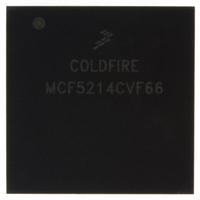
MCF5214CVF66 Freescale Semiconductor, MCF5214CVF66 Datasheet - Page 110

MCF5214CVF66
Manufacturer Part Number
MCF5214CVF66
Description
IC MPU 32BIT COLDF 256-MAPBGA
Manufacturer
Freescale Semiconductor
Series
MCF521xr
Datasheet
1.MCF5216CVM66J.pdf
(766 pages)
Specifications of MCF5214CVF66
Core Processor
Coldfire V2
Core Size
32-Bit
Speed
66MHz
Connectivity
CAN, EBI/EMI, I²C, SPI, UART/USART
Peripherals
DMA, LVD, POR, PWM, WDT
Number Of I /o
142
Program Memory Size
256KB (256K x 8)
Program Memory Type
FLASH
Ram Size
64K x 8
Voltage - Supply (vcc/vdd)
2.7 V ~ 3.6 V
Data Converters
A/D 8x12b
Oscillator Type
Internal
Operating Temperature
-40°C ~ 85°C
Package / Case
256-MAPBGA
Package
256MA-BGA
Device Core
ColdFire
Family Name
MCF521x
Maximum Speed
66 MHz
Operating Supply Voltage
3.3 V
Data Bus Width
32 Bit
Number Of Programmable I/os
142
Interface Type
QSPI/UART/I2C/CAN
On-chip Adc
8-chx10-bit
Number Of Timers
8
Lead Free Status / RoHS Status
Contains lead / RoHS non-compliant
Eeprom Size
-
Available stocks
Company
Part Number
Manufacturer
Quantity
Price
Company:
Part Number:
MCF5214CVF66
Manufacturer:
Freescale Semiconductor
Quantity:
10 000
Company:
Part Number:
MCF5214CVF66J
Manufacturer:
Freescale Semiconductor
Quantity:
10 000
- Current page: 110 of 766
- Download datasheet (9Mb)
Static RAM (SRAM)
The RAMBAR contains several control fields. These fields are shown in
5-2
31–16
15–12
11–10
Address
Bits
7–6
9
8
Reset
Reset
Field BA31 BA30 BA29 BA28 BA27 BA26 BA25 BA24 BA23 BA22 BA21 BA20 BA19 BA18 BA17 BA16
Field
R/W
R/W
31
15
PRI1, PRI2
Name
SPV
WP
BA
—
—
30
14
—
MCF5282 and MCF5216 ColdFire Microcontroller User’s Manual, Rev. 3
29
13
Figure 5-1. SRAM Base Address Register (RAMBAR)
Base address. Defines the 0-modulo-64K base address of the SRAM module. By
programming this field, the SRAM may be located on any 64-Kbyte boundary within the
processor’s 4-Gbyte address space.
Reserved, should be cleared.
Priority bit. PRI1 determines if DMA or CPU has priority in upper 32k bank of memory. PRI2
determines if DMA or CPU has priority in lower 32k bank of memory. If bit is set, CPU has
priority. If bit is cleared, DMA has priority. Priority is determined according to the following
table.
NOTE: The Freescale-recommended setting for the priority bits is 00.
Secondary port valid. Allows access by DMA
0 DMA access to memory is disabled.
1 DMA access to memory is enabled.
NOTE: The BDE bit in the second RAMBAR register must also be set to allow dual port
access to the SRAM. For more information, see
Register
Write protect. Allows only read accesses to the SRAM. When this bit is set, any attempted
write access will generate an access error exception to the ColdFire processor core.
0 Allows read and write accesses to the SRAM module
1 Allows only read accesses to the SRAM module
Reserved, should be cleared.
28
12
Table 5-1. SRAM Base Address Register
(RAMBAR).”
PRI1 PRI2 SPV
27
11
26
10
PRI[1:2]
00
01
10
11
25
9
Undefined
CPU + 0xC05
Undefined
WP
24
8
W
W
DMA Accesses
DMA Accesses
CPU Accesses
CPU Accesses
23
Upper Bank
7
Description
Priority
—
22
6
Section 8.4.2, “Memory Base Address
C/I
21
5
Figure 5-1
SC
DMA Accesses
DMA Accesses
20
CPU Accesses
CPU Accesses
4
Lower Bank
Priority
SD
19
3
Freescale Semiconductor
UC
18
2
UD
17
1
16
V
0
0
Related parts for MCF5214CVF66
Image
Part Number
Description
Manufacturer
Datasheet
Request
R
Part Number:
Description:
Manufacturer:
Freescale Semiconductor, Inc
Datasheet:
Part Number:
Description:
Manufacturer:
Freescale Semiconductor, Inc
Datasheet:
Part Number:
Description:
Manufacturer:
Freescale Semiconductor, Inc
Datasheet:
Part Number:
Description:
Manufacturer:
Freescale Semiconductor, Inc
Datasheet:
Part Number:
Description:
Manufacturer:
Freescale Semiconductor, Inc
Datasheet:
Part Number:
Description:
Manufacturer:
Freescale Semiconductor, Inc
Datasheet:
Part Number:
Description:
Manufacturer:
Freescale Semiconductor, Inc
Datasheet:
Part Number:
Description:
Manufacturer:
Freescale Semiconductor, Inc
Datasheet:
Part Number:
Description:
Manufacturer:
Freescale Semiconductor, Inc
Datasheet:
Part Number:
Description:
Manufacturer:
Freescale Semiconductor, Inc
Datasheet:
Part Number:
Description:
Manufacturer:
Freescale Semiconductor, Inc
Datasheet:
Part Number:
Description:
Manufacturer:
Freescale Semiconductor, Inc
Datasheet:
Part Number:
Description:
Manufacturer:
Freescale Semiconductor, Inc
Datasheet:
Part Number:
Description:
Manufacturer:
Freescale Semiconductor, Inc
Datasheet:
Part Number:
Description:
Manufacturer:
Freescale Semiconductor, Inc
Datasheet:


