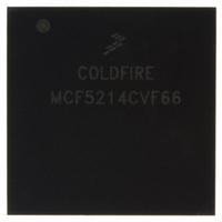
MCF5214CVF66 Freescale Semiconductor, MCF5214CVF66 Datasheet - Page 535

MCF5214CVF66
Manufacturer Part Number
MCF5214CVF66
Description
IC MPU 32BIT COLDF 256-MAPBGA
Manufacturer
Freescale Semiconductor
Series
MCF521xr
Datasheet
1.MCF5216CVM66J.pdf
(766 pages)
Specifications of MCF5214CVF66
Core Processor
Coldfire V2
Core Size
32-Bit
Speed
66MHz
Connectivity
CAN, EBI/EMI, I²C, SPI, UART/USART
Peripherals
DMA, LVD, POR, PWM, WDT
Number Of I /o
142
Program Memory Size
256KB (256K x 8)
Program Memory Type
FLASH
Ram Size
64K x 8
Voltage - Supply (vcc/vdd)
2.7 V ~ 3.6 V
Data Converters
A/D 8x12b
Oscillator Type
Internal
Operating Temperature
-40°C ~ 85°C
Package / Case
256-MAPBGA
Package
256MA-BGA
Device Core
ColdFire
Family Name
MCF521x
Maximum Speed
66 MHz
Operating Supply Voltage
3.3 V
Data Bus Width
32 Bit
Number Of Programmable I/os
142
Interface Type
QSPI/UART/I2C/CAN
On-chip Adc
8-chx10-bit
Number Of Timers
8
Lead Free Status / RoHS Status
Contains lead / RoHS non-compliant
Eeprom Size
-
Available stocks
Company
Part Number
Manufacturer
Quantity
Price
Company:
Part Number:
MCF5214CVF66
Manufacturer:
Freescale Semiconductor
Quantity:
10 000
Company:
Part Number:
MCF5214CVF66J
Manufacturer:
Freescale Semiconductor
Quantity:
10 000
- Current page: 535 of 766
- Download datasheet (9Mb)
These functions are described here.
27.6.1
During reset, the pins for the reset override functions are immediately configured to known states.
Table 27-7
If the RCON pin is not asserted during reset, the chip configuration and the reset configuration pin
functions after reset are determined by the RCON register or fixed defaults, regardless of the states of the
external data pins. The internal configuration signals are driven to levels specified by the RCON register’s
reset state for default module configuration.
If the RCON pin is asserted during reset, then various chip functions, including the reset configuration pin
functions after reset, are configured according to the levels driven onto the external data pins. (See
Table
pins to allow for module configuration.
Freescale Semiconductor
A[23:0], BS[3:0], CS[3:0]
5. Clock mode selections
6. Chip select configuration
D[31:0], R/W, TA, TEA,
TSIZ[1:0], TS, TIP, OE,
27-8) The internal configuration signals are driven to reflect the levels on the external configuration
Pin(s) Affected
Reset Configuration
shows the states of the external pins while in reset.
1
2
D[26:24, 21, 19:16],
PA[2:0], PB[5, 3:0]
RCON
CLKMOD1, CLKMOD0
During reset, the CLKMOD pins always determine the clock mode,
regardless of the RCON pin state.
If the external RCON pin is not asserted during reset, pin functions are determined by the
default operation mode defined in the RCON register. If the external RCON pin is asserted, pin
functions are determined by the override values driven on the external data bus pins.
During reset, the external RCON pin assumes its RCON pin function, but this pin changes to
the function defined by the chip operation mode immediately after reset. See
Pin
MCF5282 and MCF5216 ColdFire Microcontroller User’s Manual, Rev. 3
Table 27-7. Reset Configuration Pin States During Reset
Configuration
RCON0 = 0
Table 27-8. Configuration During Reset
Default
Digital I/O or primary
function
RCON function for all
modes
Not affected
Function
2
Pin
NOTE
Override Pins
in Reset
D[26,17:16]
100 or 0xx
1
111
110
2,34
Input
Input
Input
I/O
Output
State
—
—
—
1
Must be driven
by external logic
Internal weak
pull-up device
Must be driven by
external logic
Chip Mode Selected
Single-chip mode
Chip Configuration Module (CCM)
Table
Master mode
Input
State
Function
Reserved
27-8.
5
27-7
Related parts for MCF5214CVF66
Image
Part Number
Description
Manufacturer
Datasheet
Request
R
Part Number:
Description:
Manufacturer:
Freescale Semiconductor, Inc
Datasheet:
Part Number:
Description:
Manufacturer:
Freescale Semiconductor, Inc
Datasheet:
Part Number:
Description:
Manufacturer:
Freescale Semiconductor, Inc
Datasheet:
Part Number:
Description:
Manufacturer:
Freescale Semiconductor, Inc
Datasheet:
Part Number:
Description:
Manufacturer:
Freescale Semiconductor, Inc
Datasheet:
Part Number:
Description:
Manufacturer:
Freescale Semiconductor, Inc
Datasheet:
Part Number:
Description:
Manufacturer:
Freescale Semiconductor, Inc
Datasheet:
Part Number:
Description:
Manufacturer:
Freescale Semiconductor, Inc
Datasheet:
Part Number:
Description:
Manufacturer:
Freescale Semiconductor, Inc
Datasheet:
Part Number:
Description:
Manufacturer:
Freescale Semiconductor, Inc
Datasheet:
Part Number:
Description:
Manufacturer:
Freescale Semiconductor, Inc
Datasheet:
Part Number:
Description:
Manufacturer:
Freescale Semiconductor, Inc
Datasheet:
Part Number:
Description:
Manufacturer:
Freescale Semiconductor, Inc
Datasheet:
Part Number:
Description:
Manufacturer:
Freescale Semiconductor, Inc
Datasheet:
Part Number:
Description:
Manufacturer:
Freescale Semiconductor, Inc
Datasheet:


