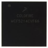
MCF5214CVF66 Freescale Semiconductor, MCF5214CVF66 Datasheet - Page 601

MCF5214CVF66
Manufacturer Part Number
MCF5214CVF66
Description
IC MPU 32BIT COLDF 256-MAPBGA
Manufacturer
Freescale Semiconductor
Series
MCF521xr
Datasheet
1.MCF5216CVM66J.pdf
(766 pages)
Specifications of MCF5214CVF66
Core Processor
Coldfire V2
Core Size
32-Bit
Speed
66MHz
Connectivity
CAN, EBI/EMI, I²C, SPI, UART/USART
Peripherals
DMA, LVD, POR, PWM, WDT
Number Of I /o
142
Program Memory Size
256KB (256K x 8)
Program Memory Type
FLASH
Ram Size
64K x 8
Voltage - Supply (vcc/vdd)
2.7 V ~ 3.6 V
Data Converters
A/D 8x12b
Oscillator Type
Internal
Operating Temperature
-40°C ~ 85°C
Package / Case
256-MAPBGA
Package
256MA-BGA
Device Core
ColdFire
Family Name
MCF521x
Maximum Speed
66 MHz
Operating Supply Voltage
3.3 V
Data Bus Width
32 Bit
Number Of Programmable I/os
142
Interface Type
QSPI/UART/I2C/CAN
On-chip Adc
8-chx10-bit
Number Of Timers
8
Lead Free Status / RoHS Status
Contains lead / RoHS non-compliant
Eeprom Size
-
Available stocks
Company
Part Number
Manufacturer
Quantity
Price
Company:
Part Number:
MCF5214CVF66
Manufacturer:
Freescale Semiconductor
Quantity:
10 000
Company:
Part Number:
MCF5214CVF66J
Manufacturer:
Freescale Semiconductor
Quantity:
10 000
- Current page: 601 of 766
- Download datasheet (9Mb)
Figure 28-50
stress conditions.
The current into the signal (I
Where:
V
V
V
R
R
The current into (I
bipolar transistor (K
I
Where:
I
A method for minimizing the impact of stress conditions on the QADC is to strategically allocate QADC
inputs so that the lower accuracy inputs are adjacent to the inputs most likely to see stress conditions.
Also, suitable source impedances should be selected to meet design goals and minimize the effect of stress
conditions.
Freescale Semiconductor
In
INJ
Stress
Selected
Stress
EB
BE
= – K
= Parasitic NPN base/emitter voltage
is either I
= Parasitic PNP emitter/base voltage
= Source impedance (10 kΩ resistor in
= Adjustable voltage source
N
= Source impedance on channel selected for conversion
* I
shows an active parasitic bipolar NPN transistor when an input signal is subjected to negative
INJ
INJN
Figure 28-51
In
or I
) the neighboring pin is determined by the K
N
‹‹ 1). The I
INJP
MCF5282 and MCF5216 ColdFire Microcontroller User’s Manual, Rev. 3
Figure 28-50. Input Signal Subjected to Negative Stress
Figure 28-51. Input Signal Subjected to Positive Stress
.
INJN
V
IN
V
IN
shows positive stress conditions can activate a similar PNP transistor.
V
or I
V
STRESS
In
STRESS
+
INJP
can be expressed by this equation:
I INJP
I INJN
+
) under negative or positive stress is determined by these equations:
=
=
R
V Stress V EB
-------------------------------------------------------------- -
R
SELECTED
–
---------------------------------------------- -
R
(
STRESS
10 kΩ
R
V Stress V BE
Figure 28-50
SELECTED
STRESS
10 kΩ
R Stress
R Stress
–
I
injP
I
IN
–
I
I
injn
IN
AN
–
AN
Parasitic
Device
AN
V DDA
AN
Parasitic
)
n+1
n
and
Device
n+1
n
Signal Under
Adjacent
Signal Under
Stress
Signal
Figure 28-51
Adjacent
N
Stress
Signal
(current coupling ratio) of the parasitic
Queued Analog-to-Digital Converter (QADC)
V
DDA
on stressed channel)
Eqn. 28-1
Eqn. 28-2
28-63
Related parts for MCF5214CVF66
Image
Part Number
Description
Manufacturer
Datasheet
Request
R
Part Number:
Description:
Manufacturer:
Freescale Semiconductor, Inc
Datasheet:
Part Number:
Description:
Manufacturer:
Freescale Semiconductor, Inc
Datasheet:
Part Number:
Description:
Manufacturer:
Freescale Semiconductor, Inc
Datasheet:
Part Number:
Description:
Manufacturer:
Freescale Semiconductor, Inc
Datasheet:
Part Number:
Description:
Manufacturer:
Freescale Semiconductor, Inc
Datasheet:
Part Number:
Description:
Manufacturer:
Freescale Semiconductor, Inc
Datasheet:
Part Number:
Description:
Manufacturer:
Freescale Semiconductor, Inc
Datasheet:
Part Number:
Description:
Manufacturer:
Freescale Semiconductor, Inc
Datasheet:
Part Number:
Description:
Manufacturer:
Freescale Semiconductor, Inc
Datasheet:
Part Number:
Description:
Manufacturer:
Freescale Semiconductor, Inc
Datasheet:
Part Number:
Description:
Manufacturer:
Freescale Semiconductor, Inc
Datasheet:
Part Number:
Description:
Manufacturer:
Freescale Semiconductor, Inc
Datasheet:
Part Number:
Description:
Manufacturer:
Freescale Semiconductor, Inc
Datasheet:
Part Number:
Description:
Manufacturer:
Freescale Semiconductor, Inc
Datasheet:
Part Number:
Description:
Manufacturer:
Freescale Semiconductor, Inc
Datasheet:


