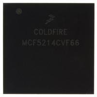
MCF5214CVF66 Freescale Semiconductor, MCF5214CVF66 Datasheet - Page 600

MCF5214CVF66
Manufacturer Part Number
MCF5214CVF66
Description
IC MPU 32BIT COLDF 256-MAPBGA
Manufacturer
Freescale Semiconductor
Series
MCF521xr
Datasheet
1.MCF5216CVM66J.pdf
(766 pages)
Specifications of MCF5214CVF66
Core Processor
Coldfire V2
Core Size
32-Bit
Speed
66MHz
Connectivity
CAN, EBI/EMI, I²C, SPI, UART/USART
Peripherals
DMA, LVD, POR, PWM, WDT
Number Of I /o
142
Program Memory Size
256KB (256K x 8)
Program Memory Type
FLASH
Ram Size
64K x 8
Voltage - Supply (vcc/vdd)
2.7 V ~ 3.6 V
Data Converters
A/D 8x12b
Oscillator Type
Internal
Operating Temperature
-40°C ~ 85°C
Package / Case
256-MAPBGA
Package
256MA-BGA
Device Core
ColdFire
Family Name
MCF521x
Maximum Speed
66 MHz
Operating Supply Voltage
3.3 V
Data Bus Width
32 Bit
Number Of Programmable I/os
142
Interface Type
QSPI/UART/I2C/CAN
On-chip Adc
8-chx10-bit
Number Of Timers
8
Lead Free Status / RoHS Status
Contains lead / RoHS non-compliant
Eeprom Size
-
Available stocks
Company
Part Number
Manufacturer
Quantity
Price
Company:
Part Number:
MCF5214CVF66
Manufacturer:
Freescale Semiconductor
Quantity:
10 000
Company:
Part Number:
MCF5214CVF66J
Manufacturer:
Freescale Semiconductor
Quantity:
10 000
- Current page: 600 of 766
- Download datasheet (9Mb)
Queued Analog-to-Digital Converter (QADC)
Other suggestions for PCB layout in which the QADC is employed include:
28.9.5
Positive or negative stress refers to conditions which exceed nominally defined operating limits. Examples
include applying a voltage exceeding the normal limit on an input (for example, voltages outside of the
suggested supply/reference ranges) or causing currents into or out of the pin which exceed normal limits.
QADC specific considerations are voltages greater than V
which cause excessive currents into or out of the input. Refer to
for more information on exact magnitudes.
Either stress conditions can potentially disrupt conversion results on neighboring inputs. Parasitic devices,
associated with CMOS processes, can cause an immediate disruptive influence on neighboring pins.
Common examples of parasitic devices are diodes to substrate and bipolar devices with the base terminal
tied to substrate (V
cause errors on the selected channel by developing a voltage drop across the selected channel’s
impedances.
28-62
•
•
•
•
•
Analog ground must be low impedance to all analog ground points in the circuit.
Bypass capacitors should be as close to the power pins as possible.
The analog ground should be isolated from the digital ground. This can be done by cutting a
separate ground plane for the analog ground.
Non-minimum traces should be utilized for connecting bypass capacitors and filters to their
corresponding ground/power points.
Minimum distance for trace runs when possible.
Accommodating Positive/Negative Stress Conditions
PCB
+5 V
SS
/V
Figure 28-49. Star-Ground at the Point of Power Supply Origin
SSA
Analog Power Supply
MCF5282 and MCF5216 ColdFire Microcontroller User’s Manual, Rev. 3
ground). Under stress conditions, current injected on an adjacent signal can
AGND
QADC
+5 V
V
V
DD
SS
DDA
or less than V
Chapter 33, “Electrical
PGND
Digital Power Supply
SSA
applied to an analog input
+5 V
Freescale Semiconductor
Characteristics”
Related parts for MCF5214CVF66
Image
Part Number
Description
Manufacturer
Datasheet
Request
R
Part Number:
Description:
Manufacturer:
Freescale Semiconductor, Inc
Datasheet:
Part Number:
Description:
Manufacturer:
Freescale Semiconductor, Inc
Datasheet:
Part Number:
Description:
Manufacturer:
Freescale Semiconductor, Inc
Datasheet:
Part Number:
Description:
Manufacturer:
Freescale Semiconductor, Inc
Datasheet:
Part Number:
Description:
Manufacturer:
Freescale Semiconductor, Inc
Datasheet:
Part Number:
Description:
Manufacturer:
Freescale Semiconductor, Inc
Datasheet:
Part Number:
Description:
Manufacturer:
Freescale Semiconductor, Inc
Datasheet:
Part Number:
Description:
Manufacturer:
Freescale Semiconductor, Inc
Datasheet:
Part Number:
Description:
Manufacturer:
Freescale Semiconductor, Inc
Datasheet:
Part Number:
Description:
Manufacturer:
Freescale Semiconductor, Inc
Datasheet:
Part Number:
Description:
Manufacturer:
Freescale Semiconductor, Inc
Datasheet:
Part Number:
Description:
Manufacturer:
Freescale Semiconductor, Inc
Datasheet:
Part Number:
Description:
Manufacturer:
Freescale Semiconductor, Inc
Datasheet:
Part Number:
Description:
Manufacturer:
Freescale Semiconductor, Inc
Datasheet:
Part Number:
Description:
Manufacturer:
Freescale Semiconductor, Inc
Datasheet:


