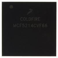
MCF5214CVF66 Freescale Semiconductor, MCF5214CVF66 Datasheet - Page 660

MCF5214CVF66
Manufacturer Part Number
MCF5214CVF66
Description
IC MPU 32BIT COLDF 256-MAPBGA
Manufacturer
Freescale Semiconductor
Series
MCF521xr
Datasheet
1.MCF5216CVM66J.pdf
(766 pages)
Specifications of MCF5214CVF66
Core Processor
Coldfire V2
Core Size
32-Bit
Speed
66MHz
Connectivity
CAN, EBI/EMI, I²C, SPI, UART/USART
Peripherals
DMA, LVD, POR, PWM, WDT
Number Of I /o
142
Program Memory Size
256KB (256K x 8)
Program Memory Type
FLASH
Ram Size
64K x 8
Voltage - Supply (vcc/vdd)
2.7 V ~ 3.6 V
Data Converters
A/D 8x12b
Oscillator Type
Internal
Operating Temperature
-40°C ~ 85°C
Package / Case
256-MAPBGA
Package
256MA-BGA
Device Core
ColdFire
Family Name
MCF521x
Maximum Speed
66 MHz
Operating Supply Voltage
3.3 V
Data Bus Width
32 Bit
Number Of Programmable I/os
142
Interface Type
QSPI/UART/I2C/CAN
On-chip Adc
8-chx10-bit
Number Of Timers
8
Lead Free Status / RoHS Status
Contains lead / RoHS non-compliant
Eeprom Size
-
Available stocks
Company
Part Number
Manufacturer
Quantity
Price
Company:
Part Number:
MCF5214CVF66
Manufacturer:
Freescale Semiconductor
Quantity:
10 000
Company:
Part Number:
MCF5214CVF66J
Manufacturer:
Freescale Semiconductor
Quantity:
10 000
- Current page: 660 of 766
- Download datasheet (9Mb)
Debug Support
Exception ProcessingPST = 0xC,{PST = 0xB,DD = destination},// stack frame
The PST/DDATA specification for the reset exception is shown below:
Exception ProcessingPST = 0xC,
The initial references at address 0 and 4 are never captured nor displayed since these accesses are treated
as instruction fetches.
30-42
1
2
3
For JMP and JSR instructions, the optional target instruction address is displayed only for those effective address
fields defining variant addressing modes. This includes the following <ea>x values: (An), (d16,An), (d8,An,Xi),
(d8,PC,Xi).
For Move Multiple instructions (MOVEM), the processor automatically generates line-sized transfers if the operand
address reaches a 0-modulo-16 boundary and there are four or more registers to be transferred. For these line-sized
transfers, the operand data is never captured nor displayed, regardless of the CSR value.
The automatic line-sized burst transfers are provided to maximize performance during these sequential memory
access operations.
During normal exception processing, the PST output is driven to a 0xC indicating the exception processing state. The
exception stack write operands, as well as the vector read and target address of the exception handler may also be
displayed.
Instruction
wddata.w
wddata.b
wddata.l
subq.l
subx.l
subi.l
swap
sub.l
sub.l
tst.w
trapf
tst.b
unlk
trap
scc
tst.l
PST = 0x5,{PST = [0x9AB],DD = target}// handler PC
PST = 0x5,{PST = [0x9AB],DD = target} // handler PC
rts
Table 30-22. PST/DDATA Specification for User-Mode Instructions (continued)
{PST = 0xB,DD = destination},// stack frame
{PST = 0xB,DD = source},// vector read
Operand Syntax
#imm,<ea>x
<ea>y,Rx
Dy,<ea>x
#imm,Dx
<ea>x
<ea>x
<ea>x
<ea>y
<ea>y
<ea>y
Dy,Dx
MCF5282 and MCF5216 ColdFire Microcontroller User’s Manual, Rev. 3
#imm
Dx
Dx
Ax
PST = 0x1, {PST = 0xB, DD = source operand},
PST = 0x5, {PST = [0x9AB], DD = target address}
PST = 0x1
PST = 0x1, {PST = 0xB, DD = source operand}
PST = 0x1, {PST = 0xB, DD = source}, {PST = 0xB, DD = destination}
PST = 0x1
PST = 0x1, {PST = 0xB, DD = source}, {PST = 0xB, DD = destination}
PST = 0x1
PST = 0x1
PST = 0x1
PST = 0x1
PST = 0x1, {PST = 0x8, DD = source operand}
PST = 0x1, {PST = 0xB, DD = source operand}
PST = 0x1, {PST = 0x9, DD = source operand}
PST = 0x1, {PST = 0xB, DD = destination operand}
PST = 0x4, {PST = 0x8, DD = source operand
PST = 0x4, {PST = 0xB, DD = source operand
PST = 0x4, {PST = 0x9, DD = source operand
3
PST/DDATA
Freescale Semiconductor
Related parts for MCF5214CVF66
Image
Part Number
Description
Manufacturer
Datasheet
Request
R
Part Number:
Description:
Manufacturer:
Freescale Semiconductor, Inc
Datasheet:
Part Number:
Description:
Manufacturer:
Freescale Semiconductor, Inc
Datasheet:
Part Number:
Description:
Manufacturer:
Freescale Semiconductor, Inc
Datasheet:
Part Number:
Description:
Manufacturer:
Freescale Semiconductor, Inc
Datasheet:
Part Number:
Description:
Manufacturer:
Freescale Semiconductor, Inc
Datasheet:
Part Number:
Description:
Manufacturer:
Freescale Semiconductor, Inc
Datasheet:
Part Number:
Description:
Manufacturer:
Freescale Semiconductor, Inc
Datasheet:
Part Number:
Description:
Manufacturer:
Freescale Semiconductor, Inc
Datasheet:
Part Number:
Description:
Manufacturer:
Freescale Semiconductor, Inc
Datasheet:
Part Number:
Description:
Manufacturer:
Freescale Semiconductor, Inc
Datasheet:
Part Number:
Description:
Manufacturer:
Freescale Semiconductor, Inc
Datasheet:
Part Number:
Description:
Manufacturer:
Freescale Semiconductor, Inc
Datasheet:
Part Number:
Description:
Manufacturer:
Freescale Semiconductor, Inc
Datasheet:
Part Number:
Description:
Manufacturer:
Freescale Semiconductor, Inc
Datasheet:
Part Number:
Description:
Manufacturer:
Freescale Semiconductor, Inc
Datasheet:


