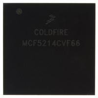
MCF5214CVF66 Freescale Semiconductor, MCF5214CVF66 Datasheet - Page 221

MCF5214CVF66
Manufacturer Part Number
MCF5214CVF66
Description
IC MPU 32BIT COLDF 256-MAPBGA
Manufacturer
Freescale Semiconductor
Series
MCF521xr
Datasheet
1.MCF5216CVM66J.pdf
(766 pages)
Specifications of MCF5214CVF66
Core Processor
Coldfire V2
Core Size
32-Bit
Speed
66MHz
Connectivity
CAN, EBI/EMI, I²C, SPI, UART/USART
Peripherals
DMA, LVD, POR, PWM, WDT
Number Of I /o
142
Program Memory Size
256KB (256K x 8)
Program Memory Type
FLASH
Ram Size
64K x 8
Voltage - Supply (vcc/vdd)
2.7 V ~ 3.6 V
Data Converters
A/D 8x12b
Oscillator Type
Internal
Operating Temperature
-40°C ~ 85°C
Package / Case
256-MAPBGA
Package
256MA-BGA
Device Core
ColdFire
Family Name
MCF521x
Maximum Speed
66 MHz
Operating Supply Voltage
3.3 V
Data Bus Width
32 Bit
Number Of Programmable I/os
142
Interface Type
QSPI/UART/I2C/CAN
On-chip Adc
8-chx10-bit
Number Of Timers
8
Lead Free Status / RoHS Status
Contains lead / RoHS non-compliant
Eeprom Size
-
Available stocks
Company
Part Number
Manufacturer
Quantity
Price
Company:
Part Number:
MCF5214CVF66
Manufacturer:
Freescale Semiconductor
Quantity:
10 000
Company:
Part Number:
MCF5214CVF66J
Manufacturer:
Freescale Semiconductor
Quantity:
10 000
- Current page: 221 of 766
- Download datasheet (9Mb)
12.4.1.3 Chip Select Control Registers (CSCR0–CSCR6)
Each CSCR, shown in
activation of each chip select. Note that to support the external boot chip select, CS0, the CSCR0 reset
values differ from the other CSCRs. CS0 allows address decoding for boot ROM before system
initialization.
Freescale Semiconductor
31–16
Bits
5–1
8
7
6
0
UC, UD
Name
BAM
SC,
WP
AM
C/I,
SD,
—
V
Base address mask. Defines the chip select block by masking address bits. Setting a BAM bit causes the
corresponding CSAR bit to be ignored in the decode.
0 Corresponding address bit is used in chip select decode.
1 Corresponding address bit is a don’t care in chip select decode.
The block size for CS[6:0] is 2
So, if CSAR0 = 0x0000 and CSMR0[BAM] = 0x0001, CS0 addresses a 128-Kbyte (2
0x0000–0x1_FFFF.
Likewise, for CS0 to access 32 Mbytes (2
CS1 to access 16 Mbytes (2
0x0000, CSMR0[BAM] = 0x01FF, CSAR1 = 0x0200, and CSMR1[BAM] = 0x00FF.
Write protect. Controls write accesses to the address range in the corresponding CSAR. Attempting to
write to the range of addresses for which CSARn[WP] = 1 results in the appropriate chip select not being
selected. No exception occurs.
0 Both read and write accesses are allowed.
1 Only read accesses are allowed.
Reserved, should be cleared.
Alternate master. When AM = 0 during a DMA access, SC, SD, UC, and UD are don’t cares in the chip
select decode.
Address space mask bits. These bits determine whether the specified accesses can occur to the address
space defined by the BAM for this chip select.
C/I
SC Supervisor code address space mask
SD Supervisor data address space mask
UC User code address space mask
UD User data address space mask
0 The address space assigned to this chip select is available to the specified access type.
1 The address space assigned to this chip select is not available (masked) to the specified access type.
Note that if AM = 0, SC, SD, UC, and UD are ignored in the chip select decode on DMA access.
Valid bit. Indicates whether the corresponding CSAR, CSMR, and CSCR contents are valid. Programmed
chip selects do not assert until V is set (except for CS0, which acts as the global chip select). Reset clears
each CSMRn[V].
0 Chip select invalid
1 Chip select valid
If this address space is accessed, chip select is not activated and a regular external bus cycle occurs.
CPU space and interrupt acknowledge cycle mask
MCF5282 and MCF5216 ColdFire Microcontroller User’s Manual, Rev. 3
Figure
12-4, controls the auto-acknowledge, port size, burst capability, and
Table 12-7. CSMRn Field Descriptions
24
n
bytes) of address space starting after the CS0 space, then CSAR0 =
where n = (number of bits set in respective CSMR[BAM]) + 16.
25
bytes) of address space starting at location 0x0000, and for
Description
17
byte) range from
Chip Select Module
12-7
Related parts for MCF5214CVF66
Image
Part Number
Description
Manufacturer
Datasheet
Request
R
Part Number:
Description:
Manufacturer:
Freescale Semiconductor, Inc
Datasheet:
Part Number:
Description:
Manufacturer:
Freescale Semiconductor, Inc
Datasheet:
Part Number:
Description:
Manufacturer:
Freescale Semiconductor, Inc
Datasheet:
Part Number:
Description:
Manufacturer:
Freescale Semiconductor, Inc
Datasheet:
Part Number:
Description:
Manufacturer:
Freescale Semiconductor, Inc
Datasheet:
Part Number:
Description:
Manufacturer:
Freescale Semiconductor, Inc
Datasheet:
Part Number:
Description:
Manufacturer:
Freescale Semiconductor, Inc
Datasheet:
Part Number:
Description:
Manufacturer:
Freescale Semiconductor, Inc
Datasheet:
Part Number:
Description:
Manufacturer:
Freescale Semiconductor, Inc
Datasheet:
Part Number:
Description:
Manufacturer:
Freescale Semiconductor, Inc
Datasheet:
Part Number:
Description:
Manufacturer:
Freescale Semiconductor, Inc
Datasheet:
Part Number:
Description:
Manufacturer:
Freescale Semiconductor, Inc
Datasheet:
Part Number:
Description:
Manufacturer:
Freescale Semiconductor, Inc
Datasheet:
Part Number:
Description:
Manufacturer:
Freescale Semiconductor, Inc
Datasheet:
Part Number:
Description:
Manufacturer:
Freescale Semiconductor, Inc
Datasheet:


