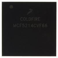
MCF5214CVF66 Freescale Semiconductor, MCF5214CVF66 Datasheet - Page 518

MCF5214CVF66
Manufacturer Part Number
MCF5214CVF66
Description
IC MPU 32BIT COLDF 256-MAPBGA
Manufacturer
Freescale Semiconductor
Series
MCF521xr
Datasheet
1.MCF5216CVM66J.pdf
(766 pages)
Specifications of MCF5214CVF66
Core Processor
Coldfire V2
Core Size
32-Bit
Speed
66MHz
Connectivity
CAN, EBI/EMI, I²C, SPI, UART/USART
Peripherals
DMA, LVD, POR, PWM, WDT
Number Of I /o
142
Program Memory Size
256KB (256K x 8)
Program Memory Type
FLASH
Ram Size
64K x 8
Voltage - Supply (vcc/vdd)
2.7 V ~ 3.6 V
Data Converters
A/D 8x12b
Oscillator Type
Internal
Operating Temperature
-40°C ~ 85°C
Package / Case
256-MAPBGA
Package
256MA-BGA
Device Core
ColdFire
Family Name
MCF521x
Maximum Speed
66 MHz
Operating Supply Voltage
3.3 V
Data Bus Width
32 Bit
Number Of Programmable I/os
142
Interface Type
QSPI/UART/I2C/CAN
On-chip Adc
8-chx10-bit
Number Of Timers
8
Lead Free Status / RoHS Status
Contains lead / RoHS non-compliant
Eeprom Size
-
Available stocks
Company
Part Number
Manufacturer
Quantity
Price
Company:
Part Number:
MCF5214CVF66
Manufacturer:
Freescale Semiconductor
Quantity:
10 000
Company:
Part Number:
MCF5214CVF66J
Manufacturer:
Freescale Semiconductor
Quantity:
10 000
- Current page: 518 of 766
- Download datasheet (9Mb)
General Purpose I/O Module
The reset values for all bits and fields in PEPAR are shown in
26-18
Bits
3–2
1-0
6
4
MCF5282 and MCF5216 ColdFire Microcontroller User’s Manual, Rev. 3
PEPA3
PEPA2
PEPA1
PEPA0
Name
Table 26-10. Reset Values for PEPAR Bits and Fields
Table 26-9. PEPAR Field Descriptions (continued)
Single chip mode
Master mode
Operation
Mode of
Port E pin assignment 3
This bit configures the port E3 pin for its alternate function
(SYNCA) or digital I/O.
1 Port E3 pin configured for alternate function (SYNCA)
0 Port E3 pin configured for digital I/O
NOTE: The SIZ1 primary function on the port E3 pin is enabled by
the SZEN bit in the CCR register. Please refer to the
“Chip Configuration Module (CCM)
configuration and the SZEN bit.
Port E pin assignment 2
This bit configures the port E2 pin for its alternate function
(SYNCB) or digital I/O.
1 Port E2 pin configured for alternate function (SYNCB)
0 Port E2 pin configured for digital I/O
NOTE: The SIZ0 primary function on the port E2 pin is enabled by
the SZEN bit in the CCR register. Please refer to the
“Chip Configuration Module
configuration and the SZEN bit.
Port E pin assignment 1.
This two-bit field in PEPAR[3:2] configures the port E1 pin for its
primary function (TS), alternate function (SYNCA), or digital I/O.
0x Port E1 pin configured for digital I/O
10 Port E1 pin configured for alternate function (SYNCA)
11 Port E1 pin configured for primary function (TS)
Port E pin assignment 0.
This two-bit field in PEPAR[1:0] configures the port E0 pin for its
primary function (TIP), alternate function (SYNCB), or digital I/O.
0x Port E0 pin configured for digital I/O
10 Port E0 pin configured for alternate function (SYNCB)
11 Port E0 pin configured for primary function (TIP)
for PEPAn Bits
(n = 2,3,4,5,6,7)
Reset Values
1
0
Description
Reset Values for
(CCM),” for more information on chip
PEPAn Fields
Table
(n = 0,1)
for more information on chip
11
00
26-10.
Chapter 27,
Chapter 27,
Freescale Semiconductor
Related parts for MCF5214CVF66
Image
Part Number
Description
Manufacturer
Datasheet
Request
R
Part Number:
Description:
Manufacturer:
Freescale Semiconductor, Inc
Datasheet:
Part Number:
Description:
Manufacturer:
Freescale Semiconductor, Inc
Datasheet:
Part Number:
Description:
Manufacturer:
Freescale Semiconductor, Inc
Datasheet:
Part Number:
Description:
Manufacturer:
Freescale Semiconductor, Inc
Datasheet:
Part Number:
Description:
Manufacturer:
Freescale Semiconductor, Inc
Datasheet:
Part Number:
Description:
Manufacturer:
Freescale Semiconductor, Inc
Datasheet:
Part Number:
Description:
Manufacturer:
Freescale Semiconductor, Inc
Datasheet:
Part Number:
Description:
Manufacturer:
Freescale Semiconductor, Inc
Datasheet:
Part Number:
Description:
Manufacturer:
Freescale Semiconductor, Inc
Datasheet:
Part Number:
Description:
Manufacturer:
Freescale Semiconductor, Inc
Datasheet:
Part Number:
Description:
Manufacturer:
Freescale Semiconductor, Inc
Datasheet:
Part Number:
Description:
Manufacturer:
Freescale Semiconductor, Inc
Datasheet:
Part Number:
Description:
Manufacturer:
Freescale Semiconductor, Inc
Datasheet:
Part Number:
Description:
Manufacturer:
Freescale Semiconductor, Inc
Datasheet:
Part Number:
Description:
Manufacturer:
Freescale Semiconductor, Inc
Datasheet:


