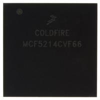
MCF5214CVF66 Freescale Semiconductor, MCF5214CVF66 Datasheet - Page 260

MCF5214CVF66
Manufacturer Part Number
MCF5214CVF66
Description
IC MPU 32BIT COLDF 256-MAPBGA
Manufacturer
Freescale Semiconductor
Series
MCF521xr
Datasheet
1.MCF5216CVM66J.pdf
(766 pages)
Specifications of MCF5214CVF66
Core Processor
Coldfire V2
Core Size
32-Bit
Speed
66MHz
Connectivity
CAN, EBI/EMI, I²C, SPI, UART/USART
Peripherals
DMA, LVD, POR, PWM, WDT
Number Of I /o
142
Program Memory Size
256KB (256K x 8)
Program Memory Type
FLASH
Ram Size
64K x 8
Voltage - Supply (vcc/vdd)
2.7 V ~ 3.6 V
Data Converters
A/D 8x12b
Oscillator Type
Internal
Operating Temperature
-40°C ~ 85°C
Package / Case
256-MAPBGA
Package
256MA-BGA
Device Core
ColdFire
Family Name
MCF521x
Maximum Speed
66 MHz
Operating Supply Voltage
3.3 V
Data Bus Width
32 Bit
Number Of Programmable I/os
142
Interface Type
QSPI/UART/I2C/CAN
On-chip Adc
8-chx10-bit
Number Of Timers
8
Lead Free Status / RoHS Status
Contains lead / RoHS non-compliant
Eeprom Size
-
Available stocks
Company
Part Number
Manufacturer
Quantity
Price
Company:
Part Number:
MCF5214CVF66
Manufacturer:
Freescale Semiconductor
Quantity:
10 000
Company:
Part Number:
MCF5214CVF66J
Manufacturer:
Freescale Semiconductor
Quantity:
10 000
- Current page: 260 of 766
- Download datasheet (9Mb)
Signal Descriptions
14.2.1.6 Transfer Error Acknowledge (TEA)
This signal indicates an error condition exists for the bus transfer. The bus cycle is terminated and the CPU
begins execution of the access error exception. This signal is an input in master mode.
This pin can also be configured as GPIO PE5.
14.2.1.7 Read/Write (R/W)
This output signal indicates the direction of the data transfer on the bus. A logic 1 indicates a read from a
slave device and a logic 0 indicates a write to a slave device.
This pin can also be configured as GPIO PE4.
14.2.1.8 Transfer Size(SIZ[1:0])
When the device is in normal mode, static bus sizing lets the programmer change data bus width between
8, 16, and 32 bits for each chip select. The SIZ[1:0] outputs specify the data access size of the current
external bus reference as shown in
Note that for misaligned transfers, SIZ[1:0] indicate the size of each transfer. For example, if a longword
access occurs at a misaligned offset of 0x1, a byte is transferred first (SIZ[1:0] = 01), a word is next
transferred at offset 0x2 (SIZ[1:0] = 10), then the final byte is transferred at offset 0x4 (SIZ[1:0] = 01).
For aligned transfers larger than the port size, SIZ[1:0] behaves as follows:
For burst-inhibited transfers, SIZ[1:0] changes with each TS assertion to reflect the next transfer size. For
transfers to port sizes smaller than the transfer size, SIZ[1:0] indicates the size of the entire transfer on the
first access and the size of the current port transfer on subsequent transfers. For example, for a longword
write to an 8-bit port, SIZ[1:0] = 00 for the first byte transfer and 01 for the next three.
These pins can also be configured as GPIO PE[3:2] or SYNCA, SYNCB.
14.2.1.9 Transfer Start (TS)
The device asserts TS during the first CLKOUT cycle of a transfer when address and attributes (TIP, R/W,
and SIZ[1:0]) are valid. TS is negated in the following CLKOUT cycle.
This pin can also be configured as GPIO PE1 or SYNCA.
14-20
•
•
If bursting is used, SIZ[1:0] stays at the size of transfer.
If bursting is inhibited, SIZ[1:0] first shows the size of the transfer and then shows the port size.
MCF5282 and MCF5216 ColdFire Microcontroller User’s Manual, Rev. 3
SIZ[1:0]
00
01
10
11
Table
Table 14-6. Transfer Size Encoding
14-6.
Transfer Size
16-byte line
Longword
Word
Byte
Freescale Semiconductor
Related parts for MCF5214CVF66
Image
Part Number
Description
Manufacturer
Datasheet
Request
R
Part Number:
Description:
Manufacturer:
Freescale Semiconductor, Inc
Datasheet:
Part Number:
Description:
Manufacturer:
Freescale Semiconductor, Inc
Datasheet:
Part Number:
Description:
Manufacturer:
Freescale Semiconductor, Inc
Datasheet:
Part Number:
Description:
Manufacturer:
Freescale Semiconductor, Inc
Datasheet:
Part Number:
Description:
Manufacturer:
Freescale Semiconductor, Inc
Datasheet:
Part Number:
Description:
Manufacturer:
Freescale Semiconductor, Inc
Datasheet:
Part Number:
Description:
Manufacturer:
Freescale Semiconductor, Inc
Datasheet:
Part Number:
Description:
Manufacturer:
Freescale Semiconductor, Inc
Datasheet:
Part Number:
Description:
Manufacturer:
Freescale Semiconductor, Inc
Datasheet:
Part Number:
Description:
Manufacturer:
Freescale Semiconductor, Inc
Datasheet:
Part Number:
Description:
Manufacturer:
Freescale Semiconductor, Inc
Datasheet:
Part Number:
Description:
Manufacturer:
Freescale Semiconductor, Inc
Datasheet:
Part Number:
Description:
Manufacturer:
Freescale Semiconductor, Inc
Datasheet:
Part Number:
Description:
Manufacturer:
Freescale Semiconductor, Inc
Datasheet:
Part Number:
Description:
Manufacturer:
Freescale Semiconductor, Inc
Datasheet:


