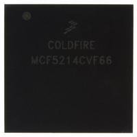
MCF5214CVF66 Freescale Semiconductor, MCF5214CVF66 Datasheet - Page 525

MCF5214CVF66
Manufacturer Part Number
MCF5214CVF66
Description
IC MPU 32BIT COLDF 256-MAPBGA
Manufacturer
Freescale Semiconductor
Series
MCF521xr
Datasheet
1.MCF5216CVM66J.pdf
(766 pages)
Specifications of MCF5214CVF66
Core Processor
Coldfire V2
Core Size
32-Bit
Speed
66MHz
Connectivity
CAN, EBI/EMI, I²C, SPI, UART/USART
Peripherals
DMA, LVD, POR, PWM, WDT
Number Of I /o
142
Program Memory Size
256KB (256K x 8)
Program Memory Type
FLASH
Ram Size
64K x 8
Voltage - Supply (vcc/vdd)
2.7 V ~ 3.6 V
Data Converters
A/D 8x12b
Oscillator Type
Internal
Operating Temperature
-40°C ~ 85°C
Package / Case
256-MAPBGA
Package
256MA-BGA
Device Core
ColdFire
Family Name
MCF521x
Maximum Speed
66 MHz
Operating Supply Voltage
3.3 V
Data Bus Width
32 Bit
Number Of Programmable I/os
142
Interface Type
QSPI/UART/I2C/CAN
On-chip Adc
8-chx10-bit
Number Of Timers
8
Lead Free Status / RoHS Status
Contains lead / RoHS non-compliant
Eeprom Size
-
Available stocks
Company
Part Number
Manufacturer
Quantity
Price
Company:
Part Number:
MCF5214CVF66
Manufacturer:
Freescale Semiconductor
Quantity:
10 000
Company:
Part Number:
MCF5214CVF66J
Manufacturer:
Freescale Semiconductor
Quantity:
10 000
- Current page: 525 of 766
- Download datasheet (9Mb)
26.3.2.14 Port TD Pin Assignment Register (PTDPAR)
The PTDPAR controls the pin function of port TD.
Freescale Semiconductor
Bits
7–6
5-4
3-2
1-0
Address
Reset
R/W:
Field
PTCPA3
PTCPA2
PTCPA1
PTCPA0
Name
7
PTDPA3
Figure 26-28. Port TD Pin Assignment Register (PTDPAR)
MCF5282 and MCF5216 ColdFire Microcontroller User’s Manual, Rev. 3
Port TC pin assignment 3. This field configures the port TC3 pin for its primary function
(DTIN3), alternate 1 function (URTS1), alternate 2 function (URTS0) or digital I/O.
00 Port TC3 pin configured for digital I/O
01 Port TC3 pin configured for alternate 2 function (URTS0)
10 Port TC3 pin configured for alternate 1 function (URTS1)
11 Port TC3 pin configured for primary function (DTIN3)
Port TC pin assignment 2. This field configures the port TC2 pin for its primary function
(DTOUT3), alternate 1 function (URTS1), alternate 2 function (URTS0) or digital I/O.
00 Port TC2 pin configured for digital I/O
01 Port TC2 pin configured for alternate 2 function (URTS0)
10 Port TC2 pin configured for alternate 1 function (URTS1)
11 Port TC2 pin configured for primary function (DTOUT3)
Port TC pin assignment 1. This field configures the port TC1 pin for its primary function
(DTIN2), alternate 1 function (UCTS1), alternate 2 function (UCTS0) or digital I/O.
00 Port TC1 pin configured for digital I/O
01 Port TC1 pin configured for alternate 2 function (UCTS0)
10 Port TC1 pin configured for alternate 1 function (UCTS1)
11 Port TC1 pin configured for primary function (DTIN2)
Port TC pin assignment 0. This field configures the port TC0 pin for its primary function
(DTOUT2), alternate 1 function (UCTS1), alternate 2 function (UCTS0) or digital I/O.
00 Port TC0 pin configured for digital I/O
01 Port TC0 pin configured for alternate 2 function (UCTS0)
10 Port TC0 pin configured for alternate 1 function (UCTS1)
11 Port TC0 pin configured for primary function (DTOUT2)
6
Table 26-17. PTCPAR Field Descriptions
5
PTDPA2
IPSBAR + 0x10_005B
4
0000_0000
R/W
Description
3
PTDPA1
2
1
General Purpose I/O Module
PTDPA0
0
26-25
Related parts for MCF5214CVF66
Image
Part Number
Description
Manufacturer
Datasheet
Request
R
Part Number:
Description:
Manufacturer:
Freescale Semiconductor, Inc
Datasheet:
Part Number:
Description:
Manufacturer:
Freescale Semiconductor, Inc
Datasheet:
Part Number:
Description:
Manufacturer:
Freescale Semiconductor, Inc
Datasheet:
Part Number:
Description:
Manufacturer:
Freescale Semiconductor, Inc
Datasheet:
Part Number:
Description:
Manufacturer:
Freescale Semiconductor, Inc
Datasheet:
Part Number:
Description:
Manufacturer:
Freescale Semiconductor, Inc
Datasheet:
Part Number:
Description:
Manufacturer:
Freescale Semiconductor, Inc
Datasheet:
Part Number:
Description:
Manufacturer:
Freescale Semiconductor, Inc
Datasheet:
Part Number:
Description:
Manufacturer:
Freescale Semiconductor, Inc
Datasheet:
Part Number:
Description:
Manufacturer:
Freescale Semiconductor, Inc
Datasheet:
Part Number:
Description:
Manufacturer:
Freescale Semiconductor, Inc
Datasheet:
Part Number:
Description:
Manufacturer:
Freescale Semiconductor, Inc
Datasheet:
Part Number:
Description:
Manufacturer:
Freescale Semiconductor, Inc
Datasheet:
Part Number:
Description:
Manufacturer:
Freescale Semiconductor, Inc
Datasheet:
Part Number:
Description:
Manufacturer:
Freescale Semiconductor, Inc
Datasheet:


