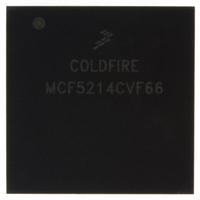
MCF5214CVF66 Freescale Semiconductor, MCF5214CVF66 Datasheet - Page 234

MCF5214CVF66
Manufacturer Part Number
MCF5214CVF66
Description
IC MPU 32BIT COLDF 256-MAPBGA
Manufacturer
Freescale Semiconductor
Series
MCF521xr
Datasheet
1.MCF5216CVM66J.pdf
(766 pages)
Specifications of MCF5214CVF66
Core Processor
Coldfire V2
Core Size
32-Bit
Speed
66MHz
Connectivity
CAN, EBI/EMI, I²C, SPI, UART/USART
Peripherals
DMA, LVD, POR, PWM, WDT
Number Of I /o
142
Program Memory Size
256KB (256K x 8)
Program Memory Type
FLASH
Ram Size
64K x 8
Voltage - Supply (vcc/vdd)
2.7 V ~ 3.6 V
Data Converters
A/D 8x12b
Oscillator Type
Internal
Operating Temperature
-40°C ~ 85°C
Package / Case
256-MAPBGA
Package
256MA-BGA
Device Core
ColdFire
Family Name
MCF521x
Maximum Speed
66 MHz
Operating Supply Voltage
3.3 V
Data Bus Width
32 Bit
Number Of Programmable I/os
142
Interface Type
QSPI/UART/I2C/CAN
On-chip Adc
8-chx10-bit
Number Of Timers
8
Lead Free Status / RoHS Status
Contains lead / RoHS non-compliant
Eeprom Size
-
Available stocks
Company
Part Number
Manufacturer
Quantity
Price
Company:
Part Number:
MCF5214CVF66
Manufacturer:
Freescale Semiconductor
Quantity:
10 000
Company:
Part Number:
MCF5214CVF66J
Manufacturer:
Freescale Semiconductor
Quantity:
10 000
- Current page: 234 of 766
- Download datasheet (9Mb)
External Interface Module (EIM)
13.4.7
The processor can be programmed to initiate burst cycles if its transfer size exceeds the size of the port it
is transferring to. For example, a word transfer to an 8-bit port would take a 2-byte burst cycle. A line
transfer to a 32-bit port would take a 4-longword burst cycle.
The external bus can support 2-1-1-1 burst cycles to maximize cache performance and optimize DMA
transfers. A user can add wait states by delaying termination of the cycle. The initiation of a burst cycle is
encoded on the size pins. For burst transfers to smaller port sizes, SIZ[1:0] indicates the size of the entire
transfer. For example, if the processor writes a longword to an 8-bit port, SIZ[1:0] = 00 for the first byte
transfer and does not change.
The CSCRs can be used to enable bursting for reads, writes, or both. Processor memory space can be
declared burst-inhibited for reads and writes by clearing the appropriate CSCRn[BSTR,BSTW]. A line
access to a burst-inhibited region first accesses the processor bus encoded as a line access. The SIZ[1:0]
encoding does not exceed the programmed port size. The address changes if internal termination is used
but does not change if external termination is used, as shown in
13.4.7.1 Line Transfers
A line is a 16-byte-aligned, 16-byte value. Despite the alignment, a line access may not begin on the
aligned address; therefore, the bus interface supports line transfers on multiple address boundaries.
Table 13-4
13.4.7.2 Line Read Bus Cycles
Figure 13-12
read bus cycle with the first data transfer sampled on the rising edge of S4, but the next pipelined burst
data is sampled a cycle later on the rising edge of S6. Each subsequent pipelined data burst is single cycle
until the last one, which can be held for up to two CLKOUT cycles after TA is asserted. Note that CSn are
asserted throughout the burst transfer. This example shows the timing for external termination, which
differs from the internal termination example in
the beginning (assertion of TS and TIP) and end (negation of TIP) of the transfer.
13-10
Burst Cycles
shows allowable patterns for line accesses.
and
Figure 13-13
MCF5282 and MCF5216 ColdFire Microcontroller User’s Manual, Rev. 3
Table 13-4. Allowable Line Access Patterns
show a line access read with zero wait states. The access starts like a basic
A[3:2]
00
01
10
11
Figure 13-13
Longword Accesses
only in that the address lines change only at
0–4–8–C
4–8–C–0
8–C–0–4
C–0–4–8
Figure 13-12
and
Figure
Freescale Semiconductor
13-13.
Related parts for MCF5214CVF66
Image
Part Number
Description
Manufacturer
Datasheet
Request
R
Part Number:
Description:
Manufacturer:
Freescale Semiconductor, Inc
Datasheet:
Part Number:
Description:
Manufacturer:
Freescale Semiconductor, Inc
Datasheet:
Part Number:
Description:
Manufacturer:
Freescale Semiconductor, Inc
Datasheet:
Part Number:
Description:
Manufacturer:
Freescale Semiconductor, Inc
Datasheet:
Part Number:
Description:
Manufacturer:
Freescale Semiconductor, Inc
Datasheet:
Part Number:
Description:
Manufacturer:
Freescale Semiconductor, Inc
Datasheet:
Part Number:
Description:
Manufacturer:
Freescale Semiconductor, Inc
Datasheet:
Part Number:
Description:
Manufacturer:
Freescale Semiconductor, Inc
Datasheet:
Part Number:
Description:
Manufacturer:
Freescale Semiconductor, Inc
Datasheet:
Part Number:
Description:
Manufacturer:
Freescale Semiconductor, Inc
Datasheet:
Part Number:
Description:
Manufacturer:
Freescale Semiconductor, Inc
Datasheet:
Part Number:
Description:
Manufacturer:
Freescale Semiconductor, Inc
Datasheet:
Part Number:
Description:
Manufacturer:
Freescale Semiconductor, Inc
Datasheet:
Part Number:
Description:
Manufacturer:
Freescale Semiconductor, Inc
Datasheet:
Part Number:
Description:
Manufacturer:
Freescale Semiconductor, Inc
Datasheet:


