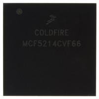
MCF5214CVF66 Freescale Semiconductor, MCF5214CVF66 Datasheet - Page 544

MCF5214CVF66
Manufacturer Part Number
MCF5214CVF66
Description
IC MPU 32BIT COLDF 256-MAPBGA
Manufacturer
Freescale Semiconductor
Series
MCF521xr
Datasheet
1.MCF5216CVM66J.pdf
(766 pages)
Specifications of MCF5214CVF66
Core Processor
Coldfire V2
Core Size
32-Bit
Speed
66MHz
Connectivity
CAN, EBI/EMI, I²C, SPI, UART/USART
Peripherals
DMA, LVD, POR, PWM, WDT
Number Of I /o
142
Program Memory Size
256KB (256K x 8)
Program Memory Type
FLASH
Ram Size
64K x 8
Voltage - Supply (vcc/vdd)
2.7 V ~ 3.6 V
Data Converters
A/D 8x12b
Oscillator Type
Internal
Operating Temperature
-40°C ~ 85°C
Package / Case
256-MAPBGA
Package
256MA-BGA
Device Core
ColdFire
Family Name
MCF521x
Maximum Speed
66 MHz
Operating Supply Voltage
3.3 V
Data Bus Width
32 Bit
Number Of Programmable I/os
142
Interface Type
QSPI/UART/I2C/CAN
On-chip Adc
8-chx10-bit
Number Of Timers
8
Lead Free Status / RoHS Status
Contains lead / RoHS non-compliant
Eeprom Size
-
Available stocks
Company
Part Number
Manufacturer
Quantity
Price
Company:
Part Number:
MCF5214CVF66
Manufacturer:
Freescale Semiconductor
Quantity:
10 000
Company:
Part Number:
MCF5214CVF66J
Manufacturer:
Freescale Semiconductor
Quantity:
10 000
- Current page: 544 of 766
- Download datasheet (9Mb)
Queued Analog-to-Digital Converter (QADC)
28.4.6
V
reference inputs from the power supply signals allows for additional external filtering, which increases
reference voltage precision and stability, and subsequently contributes to a higher degree of conversion
accuracy.
28.4.7
The V
power is required to isolate the sensitive analog circuitry from the normal levels of noise present on the
digital power supply.
28.4.8
V
signals to tolerate 5 volts when configured as inputs and drive 5 volts when configured as outputs.
28.5
The QADC occupies 1 Kbyte, or 512 half-word (16-bit) entries, of address space. Ten half-word registers
are control, port, and status registers, 64 half-word entries are the CCW table, and 64 half-word entries are
the result table which occupies 192 half-word address locations because the result data is readable in three
data alignment formats.
28-6
RH
DDH
and V
DDA
provides 5-V power to the digital I/O functions of QADC port QA and port QB. This allows those
0x19_0000
0x19_0002
0x19_0004
0x19_0006
0x19_0008
0x19_000a
0x19_000c
0x19_000e
0x19_0010
0x19_0012
IPSBAR +
Memory Map
Offset
Voltage Reference Signals
Dedicated Analog Supply Signals
Dedicated Digital I/O Port Supply Signal
and V
RL
V
more
Considerations.
are the dedicated input signals for the high and low reference voltages. Separating the
RH
SSA
and V
signals supply power to the analog subsystems of the QADC module. Dedicated
information,
Table 28-2
Port QA Data Register (PORTQA)
MCF5282 and MCF5216 ColdFire Microcontroller User’s Manual, Rev. 3
Port QA Data Direction Register
RL
must be set to V
QADC Module Configuration Register (QADCMCR)
(DDRQA)
is the QADC memory map.
MSB
Table 28-2. QADC Memory Map
refer
QADC Test Register (QADCTEST)
QADC Control Register 0 (QACR0)
QADC Control Register 1 (QACR1)
QADC Control Register 2 (QACR2)
QADC Status Register 0 (QASR0)
QADC Status Register 1 (QASR1)
to
DDA
NOTE
Reserved
Section 28.9,
and V
Port QB Data Register (PORTQB)
SSA
Port QB Data Direction Register
3
potential, respectively. For
“Signal
(DDRQB)
2
LSB
Connection
Freescale Semiconductor
Access
S/U
S/U
S/U
S/U
S/U
S/U
S/U
—
S
S
1
Related parts for MCF5214CVF66
Image
Part Number
Description
Manufacturer
Datasheet
Request
R
Part Number:
Description:
Manufacturer:
Freescale Semiconductor, Inc
Datasheet:
Part Number:
Description:
Manufacturer:
Freescale Semiconductor, Inc
Datasheet:
Part Number:
Description:
Manufacturer:
Freescale Semiconductor, Inc
Datasheet:
Part Number:
Description:
Manufacturer:
Freescale Semiconductor, Inc
Datasheet:
Part Number:
Description:
Manufacturer:
Freescale Semiconductor, Inc
Datasheet:
Part Number:
Description:
Manufacturer:
Freescale Semiconductor, Inc
Datasheet:
Part Number:
Description:
Manufacturer:
Freescale Semiconductor, Inc
Datasheet:
Part Number:
Description:
Manufacturer:
Freescale Semiconductor, Inc
Datasheet:
Part Number:
Description:
Manufacturer:
Freescale Semiconductor, Inc
Datasheet:
Part Number:
Description:
Manufacturer:
Freescale Semiconductor, Inc
Datasheet:
Part Number:
Description:
Manufacturer:
Freescale Semiconductor, Inc
Datasheet:
Part Number:
Description:
Manufacturer:
Freescale Semiconductor, Inc
Datasheet:
Part Number:
Description:
Manufacturer:
Freescale Semiconductor, Inc
Datasheet:
Part Number:
Description:
Manufacturer:
Freescale Semiconductor, Inc
Datasheet:
Part Number:
Description:
Manufacturer:
Freescale Semiconductor, Inc
Datasheet:


