DF2398F20V Renesas Electronics America, DF2398F20V Datasheet - Page 146
DF2398F20V
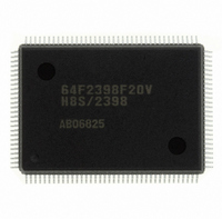
Manufacturer Part Number
DF2398F20V
Description
IC H8S/2300 MCU FLASH 128QFP
Manufacturer
Renesas Electronics America
Series
H8® H8S/2300r
Specifications of DF2398F20V
Core Processor
H8S/2000
Core Size
16-Bit
Speed
20MHz
Connectivity
SCI, SmartCard
Peripherals
DMA, POR, PWM, WDT
Number Of I /o
87
Program Memory Size
256KB (256K x 8)
Program Memory Type
FLASH
Ram Size
8K x 8
Voltage - Supply (vcc/vdd)
4.5 V ~ 5.5 V
Data Converters
A/D 8x10b; D/A 2x8b
Oscillator Type
Internal
Operating Temperature
-20°C ~ 75°C
Package / Case
128-QFP
For Use With
YR0K42378FC000BA - KIT EVAL FOR H8S/2378
Lead Free Status / RoHS Status
Lead free / RoHS Compliant
Eeprom Size
-
Available stocks
Company
Part Number
Manufacturer
Quantity
Price
Company:

Part Number:
DF2398F20V
Manufacturer:
Renesas Electronics America
Quantity:
135
Company:
Part Number:
DF2398F20V
Manufacturer:
Renesas Electronics America
Quantity:
10 000


Bit 0—WAIT Pin Enable (WAITE): Selects enabling or disabling of wait input by the WAIT pin.
6.2.6
MCR is an 8-bit readable/writable register that selects the DRAM strobe control method, number of precharge cycles,
access mode, address multiplexing shift size, and the number of wait states inserted during refreshing, when areas 2 to 5
are designated as DRAM interface.
MCR is initialized to H'00 by a power-on reset and in hardware standby mode. It is not initialized by a manual reset* or in
software standby mode.
Note: * Manual reset is only supported in the H8S/2357 ZTAT.
Bit 7—TP Cycle Control (TPC): Selects whether a 1-state or 2-state precharge cycle (T
designated as DRAM space are accessed.
Bit 6—Burst Access Enable (BE): Selects enabling or disabling of burst access to areas 2 to 5 designated as DRAM
space. DRAM space burst access is performed in fast page mode.
Bit 5—RAS Down Mode (RCDM): When areas 2 to 5 are designated as DRAM space and access to DRAM is
interrupted, RCDM selects whether the next DRAM access is waited for with the RAS signal held low (RAS down mode),
or the RAS signal is driven high again (RAS up mode).
Rev.6.00 Oct.28.2004 page 116 of 1016
REJ09B0138-0600H
Bit
Initial value :
R/W
Memory Control Register (MCR)
Bit 0
WAITE
0
1
Bit 7
TPC
0
1
Bit 6
BE
0
1
Bit 5
RCDM
0
1
:
:
TPC
R/W
7
0
Description
Wait input by WAIT pin disabled. WAIT pin can be used as I/O port.
Wait input by WAIT pin enabled
Description
1-state precharge cycle is inserted
2-state precharge cycle is inserted
Description
Burst disabled (always full access)
For DRAM space access, access in fast page mode
Description
DRAM interface: RAS up mode selected
DRAM interface: RAS down mode selected
R/W
BE
6
0
RCDM
R/W
5
0
CW2
R/W
4
0
MXC1
R/W
3
0
MXC0
R/W
2
0
RLW1
R/W
1
0
P
) is to be used when areas 2 to 5
RLW0
R/W
0
0
(Initial value)
(Initial value)
(Initial value)
(Initial value)
Related parts for DF2398F20V
Image
Part Number
Description
Manufacturer
Datasheet
Request
R

Part Number:
Description:
CONN PLUG 12POS DUAL 0.5MM SMD
Manufacturer:
Hirose Electric Co Ltd
Datasheet:
Part Number:
Description:
CONN PLUG 18POS DUAL 0.5MM SMD
Manufacturer:
Hirose Electric Co Ltd
Datasheet:
Part Number:
Description:
CONN PLUG 14POS DUAL 0.5MM SMD
Manufacturer:
Hirose Electric Co Ltd
Datasheet:
Part Number:
Description:
CONN RECEPT 20POS DUAL 0.5MM SMD
Manufacturer:
Hirose Electric Co Ltd
Datasheet:
Part Number:
Description:
CONN PLUG 16POS DUAL 0.5MM SMD
Manufacturer:
Hirose Electric Co Ltd
Datasheet:
Part Number:
Description:
CONN RECEPT 16POS DUAL 0.5MM SMD
Manufacturer:
Hirose Electric Co Ltd
Datasheet:
Part Number:
Description:
CONN PLUG 20POS DUAL 0.5MM SMD
Manufacturer:
Hirose Electric Co Ltd
Datasheet:
Part Number:
Description:
CONN PLUG 30POS DUAL 0.5MM SMD
Manufacturer:
Hirose Electric Co Ltd
Datasheet:
Part Number:
Description:
CONN RECEPT 30POS DUAL 0.5MM SMD
Manufacturer:
Hirose Electric Co Ltd
Datasheet:
Part Number:
Description:
CONN PLUG 40POS DUAL 0.5MM SMD
Manufacturer:
Hirose Electric Co Ltd
Datasheet:

Part Number:
Description:
KIT STARTER FOR M16C/29
Manufacturer:
Renesas Electronics America
Datasheet:

Part Number:
Description:
KIT STARTER FOR R8C/2D
Manufacturer:
Renesas Electronics America
Datasheet:

Part Number:
Description:
R0K33062P STARTER KIT
Manufacturer:
Renesas Electronics America
Datasheet:

Part Number:
Description:
KIT STARTER FOR R8C/23 E8A
Manufacturer:
Renesas Electronics America
Datasheet:

Part Number:
Description:
KIT STARTER FOR R8C/25
Manufacturer:
Renesas Electronics America
Datasheet: