DF2398F20V Renesas Electronics America, DF2398F20V Datasheet - Page 574
DF2398F20V
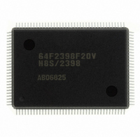
Manufacturer Part Number
DF2398F20V
Description
IC H8S/2300 MCU FLASH 128QFP
Manufacturer
Renesas Electronics America
Series
H8® H8S/2300r
Specifications of DF2398F20V
Core Processor
H8S/2000
Core Size
16-Bit
Speed
20MHz
Connectivity
SCI, SmartCard
Peripherals
DMA, POR, PWM, WDT
Number Of I /o
87
Program Memory Size
256KB (256K x 8)
Program Memory Type
FLASH
Ram Size
8K x 8
Voltage - Supply (vcc/vdd)
4.5 V ~ 5.5 V
Data Converters
A/D 8x10b; D/A 2x8b
Oscillator Type
Internal
Operating Temperature
-20°C ~ 75°C
Package / Case
128-QFP
For Use With
YR0K42378FC000BA - KIT EVAL FOR H8S/2378
Lead Free Status / RoHS Status
Lead free / RoHS Compliant
Eeprom Size
-
Available stocks
Company
Part Number
Manufacturer
Quantity
Price
Company:

Part Number:
DF2398F20V
Manufacturer:
Renesas Electronics America
Quantity:
135
Company:
Part Number:
DF2398F20V
Manufacturer:
Renesas Electronics America
Quantity:
10 000


Bits 2 to 0—Channel Select 2 to 0 (CH2 to CH0): Together with the SCAN bit, these bits select the analog input
channels.
Only set the input channel while conversion is stopped (ADST = 0).
16.2.3
Note: * Applies to the H8S/2398, H8S/2394, H8S/2392, and H8S/2390.
ADCR is an 8-bit readable/writable register that enables or disables external triggering of A/D conversion operations.
ADCR is initialized to H'3F by a reset, and in standby mode or module stop mode.
Bits 7 and 6—Timer Trigger Select 1 and 0 (TRGS1, TRGS0): Select enabling or disabling of the start of A/D
conversion by a trigger signal. Only set bits TRGS1 and TRGS0 while conversion is stopped (ADST = 0).
(1) For H8S/2357 and H8S/2352
Bits 5 to 0—Reserved: They are always read as 1 and cannot be modified.
(2) For H8S/2398, H8S/2394, H8S/2392, and H8S/2390
Bits 5, 4, 1, and 0—Reserved: They are always read as 1 and cannot be modified.
Bits 3 and 2—Reserved: Should always be written with 1.
Rev.6.00 Oct.28.2004 page 544 of 1016
REJ09B0138-0600H
Bit
Initial value :
R/W
A/D Control Register (ADCR)
Bit 7
TRGS1
0
1
Group
Selection
CH2
0
1
:
:
TRGS1
R/W
7
0
Bit 6
TRGS0
0
1
0
1
CH1
0
1
0
1
TRGS0
R/W
Channel Selection
6
0
Description
A/D conversion start by external trigger is disabled
A/D conversion start by external trigger (TPU) is enabled
A/D conversion start by external trigger (8-bit timer) is enabled
A/D conversion start by external trigger pin (ADTRG) is enabled
—
—
5
1
CH0
0
1
0
1
0
1
0
1
—
—
4
1
Single Mode (SCAN=0)
AN0 (Initial value)
AN1
AN2
AN3
AN4
AN5
AN6
AN7
—/(R/W)* —/(R/W)*
—
3
1
—
2
1
Description
—
—
1
1
Scan Mode (SCAN=1)
AN0
AN0, AN1
AN0 to AN2
AN0 to AN3
AN4
AN4, AN5
AN4 to AN6
AN4 to AN7
—
—
0
1
(Initial value)
Related parts for DF2398F20V
Image
Part Number
Description
Manufacturer
Datasheet
Request
R

Part Number:
Description:
CONN PLUG 12POS DUAL 0.5MM SMD
Manufacturer:
Hirose Electric Co Ltd
Datasheet:
Part Number:
Description:
CONN PLUG 18POS DUAL 0.5MM SMD
Manufacturer:
Hirose Electric Co Ltd
Datasheet:
Part Number:
Description:
CONN PLUG 14POS DUAL 0.5MM SMD
Manufacturer:
Hirose Electric Co Ltd
Datasheet:
Part Number:
Description:
CONN RECEPT 20POS DUAL 0.5MM SMD
Manufacturer:
Hirose Electric Co Ltd
Datasheet:
Part Number:
Description:
CONN PLUG 16POS DUAL 0.5MM SMD
Manufacturer:
Hirose Electric Co Ltd
Datasheet:
Part Number:
Description:
CONN RECEPT 16POS DUAL 0.5MM SMD
Manufacturer:
Hirose Electric Co Ltd
Datasheet:
Part Number:
Description:
CONN PLUG 20POS DUAL 0.5MM SMD
Manufacturer:
Hirose Electric Co Ltd
Datasheet:
Part Number:
Description:
CONN PLUG 30POS DUAL 0.5MM SMD
Manufacturer:
Hirose Electric Co Ltd
Datasheet:
Part Number:
Description:
CONN RECEPT 30POS DUAL 0.5MM SMD
Manufacturer:
Hirose Electric Co Ltd
Datasheet:
Part Number:
Description:
CONN PLUG 40POS DUAL 0.5MM SMD
Manufacturer:
Hirose Electric Co Ltd
Datasheet:

Part Number:
Description:
KIT STARTER FOR M16C/29
Manufacturer:
Renesas Electronics America
Datasheet:

Part Number:
Description:
KIT STARTER FOR R8C/2D
Manufacturer:
Renesas Electronics America
Datasheet:

Part Number:
Description:
R0K33062P STARTER KIT
Manufacturer:
Renesas Electronics America
Datasheet:

Part Number:
Description:
KIT STARTER FOR R8C/23 E8A
Manufacturer:
Renesas Electronics America
Datasheet:

Part Number:
Description:
KIT STARTER FOR R8C/25
Manufacturer:
Renesas Electronics America
Datasheet: