DF2398F20V Renesas Electronics America, DF2398F20V Datasheet - Page 761
DF2398F20V
Manufacturer Part Number
DF2398F20V
Description
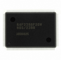
IC H8S/2300 MCU FLASH 128QFP
Manufacturer
Renesas Electronics America
Series
H8® H8S/2300r
Specifications of DF2398F20V
Core Processor
H8S/2000
Core Size
16-Bit
Speed
20MHz
Connectivity
SCI, SmartCard
Peripherals
DMA, POR, PWM, WDT
Number Of I /o
87
Program Memory Size
256KB (256K x 8)
Program Memory Type
FLASH
Ram Size
8K x 8
Voltage - Supply (vcc/vdd)
4.5 V ~ 5.5 V
Data Converters
A/D 8x10b; D/A 2x8b
Oscillator Type
Internal
Operating Temperature
-20°C ~ 75°C
Package / Case
128-QFP
For Use With
YR0K42378FC000BA - KIT EVAL FOR H8S/2378
Lead Free Status / RoHS Status
Lead free / RoHS Compliant
Eeprom Size
-
Available stocks
Company
Part Number
Manufacturer
Quantity
Price
Company:

Part Number:
DF2398F20V
Manufacturer:
Renesas Electronics America
Quantity:
135
Company:
Part Number:
DF2398F20V
Manufacturer:
Renesas Electronics America
Quantity:
10 000


Notes: 1. If the A/D and D/A converters are not used, do not leave the AV
Table 22-24 DC Characteristics (3)
Conditions: V
2. Current dissipation values are for V
3. The values are for V
4. I
Connect AV
on-chip pull-up transistors in the off state.
I
I
Item
Current
dissipation*
Analog power
supply current
Reference
current
RAM standby voltage
Item
Schmitt
trigger input
voltage
Input high
voltage
Input low
voltage
T
CC
CC
CC
a
CC
depends on V
max = 1.0 (mA) + 1.1 (mA/(MHz
max = 1.0 (mA) + 0.75 (mA/(MHz
= –20 to +75 C (regular specifications), T
= 3.0 to 5.5 V, AV
CC
2
and V
Port 2,
P6
PA
RES, STBY,
NMI, MD
to MD
EXTAL
Ports 1, 3, 5,
B to G,
P6
PA
Port 4
RES, STBY,
MD
NMI, EXTAL,
Ports 1, 3 to 5,
B to G,
P6
PA
Normal
operation
Sleep mode
Standby
mode*
During A/D
and D/A
conversion
Idle
During A/D
and D/A
conversion
Idle
CC
4
0
0
4
0
0
and f as follows:
ref
RAM
2
to P6
to P6
to P6
to PA
to PA
to PA
to MD
to V
0
3
CC
V
2
7
3
3
CC
7
3
3
= 3.0 to 5.5 V, V
,
,
,
CC
0
, and connect AV
< 2.7 V, V
Symbol
I
Al
Al
V
Symbol
V
V
V
V
V
CC
RAM
T
T
T
IH
IL
–
+
+
CC
CC
*
IH
– V
4
min = V
V))
V))
T
IH
–
min = V
—
—
Min
—
—
—
—
—
—
2.0
Min
V
—
V
V
V
V
V
–0.3
–0.3
V
ref
CC
CC
CC
CC
CC
CC
V
CC
CC
SS
a
= 3.0 V to AV
CC
–0.5 V and V
= –40 to +85 C (wide-range specifications)
to V
0.2
0.07
0.9 —
0.7 —
0.7 —
0.7 —
CC
f [normal mode]
f [sleep mode]
SS
0.9, and V
.
Typ
23
(3.0 V)
16
(3.0 V)
0.01
—
0.2
(3.0 V)
0.01
1.4
(3.0 V)
0.01
—
Typ
—
—
—
—
—
IL
CC
Max
62
42
5.0
20.0
2.0
5.0
3.0
5.0
—
Max
—
V
—
V
V
V
AV
V
V
0.8
max = 0.5 V with all output pins unloaded and the
, V
CC
CC
CC
CC
CC
CC
CC
IL
CC
, AV
max = 0.3 V.
SS
+0.3
+0.3
+0.3
+0.3 V
0.7
0.1 V
0.2 V
= AV
SS
, and V
Rev.6.00 Oct.28.2004 page 731 of 1016
Unit
mA
mA
mA
mA
V
Unit
V
V
V
V
V
V
SS
A
A
A
= 0 V*
ref
pins open.
Test Conditions
f = 10 MHz
f = 10 MHz
T
50 C < T
Test Conditions
V
V
a
CC
CC
1
,
< 4.0 V
= 4.0 to 5.5 V
50 C
a
REJ09B0138-0600H
Related parts for DF2398F20V
Image
Part Number
Description
Manufacturer
Datasheet
Request
R

Part Number:
Description:
CONN PLUG 12POS DUAL 0.5MM SMD
Manufacturer:
Hirose Electric Co Ltd
Datasheet:
Part Number:
Description:
CONN PLUG 18POS DUAL 0.5MM SMD
Manufacturer:
Hirose Electric Co Ltd
Datasheet:
Part Number:
Description:
CONN PLUG 14POS DUAL 0.5MM SMD
Manufacturer:
Hirose Electric Co Ltd
Datasheet:
Part Number:
Description:
CONN RECEPT 20POS DUAL 0.5MM SMD
Manufacturer:
Hirose Electric Co Ltd
Datasheet:
Part Number:
Description:
CONN PLUG 16POS DUAL 0.5MM SMD
Manufacturer:
Hirose Electric Co Ltd
Datasheet:
Part Number:
Description:
CONN RECEPT 16POS DUAL 0.5MM SMD
Manufacturer:
Hirose Electric Co Ltd
Datasheet:
Part Number:
Description:
CONN PLUG 20POS DUAL 0.5MM SMD
Manufacturer:
Hirose Electric Co Ltd
Datasheet:
Part Number:
Description:
CONN PLUG 30POS DUAL 0.5MM SMD
Manufacturer:
Hirose Electric Co Ltd
Datasheet:
Part Number:
Description:
CONN RECEPT 30POS DUAL 0.5MM SMD
Manufacturer:
Hirose Electric Co Ltd
Datasheet:
Part Number:
Description:
CONN PLUG 40POS DUAL 0.5MM SMD
Manufacturer:
Hirose Electric Co Ltd
Datasheet:

Part Number:
Description:
KIT STARTER FOR M16C/29
Manufacturer:
Renesas Electronics America
Datasheet:

Part Number:
Description:
KIT STARTER FOR R8C/2D
Manufacturer:
Renesas Electronics America
Datasheet:

Part Number:
Description:
R0K33062P STARTER KIT
Manufacturer:
Renesas Electronics America
Datasheet:

Part Number:
Description:
KIT STARTER FOR R8C/23 E8A
Manufacturer:
Renesas Electronics America
Datasheet:

Part Number:
Description:
KIT STARTER FOR R8C/25
Manufacturer:
Renesas Electronics America
Datasheet: