DF2398F20V Renesas Electronics America, DF2398F20V Datasheet - Page 448
DF2398F20V
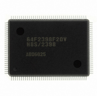
Manufacturer Part Number
DF2398F20V
Description
IC H8S/2300 MCU FLASH 128QFP
Manufacturer
Renesas Electronics America
Series
H8® H8S/2300r
Specifications of DF2398F20V
Core Processor
H8S/2000
Core Size
16-Bit
Speed
20MHz
Connectivity
SCI, SmartCard
Peripherals
DMA, POR, PWM, WDT
Number Of I /o
87
Program Memory Size
256KB (256K x 8)
Program Memory Type
FLASH
Ram Size
8K x 8
Voltage - Supply (vcc/vdd)
4.5 V ~ 5.5 V
Data Converters
A/D 8x10b; D/A 2x8b
Oscillator Type
Internal
Operating Temperature
-20°C ~ 75°C
Package / Case
128-QFP
For Use With
YR0K42378FC000BA - KIT EVAL FOR H8S/2378
Lead Free Status / RoHS Status
Lead free / RoHS Compliant
Eeprom Size
-
Available stocks
Company
Part Number
Manufacturer
Quantity
Price
Company:

Part Number:
DF2398F20V
Manufacturer:
Renesas Electronics America
Quantity:
135
Company:
Part Number:
DF2398F20V
Manufacturer:
Renesas Electronics America
Quantity:
10 000


Address H'FF4D
Address H'FF4F
11.2.5
PCR is an 8-bit readable/writable register that selects output trigger signals for PPG outputs on a group-by-group basis.
PCR is initialized to H'FF by a reset and in hardware standby mode. It is not initialized in software standby mode.
Bits 7 and 6—Group 3 Compare Match Select 1 and 0 (G3CMS1, G3CMS0): These bits select the compare match
that triggers pulse output group 3 (pins PO15 to PO12).
Bits 5 and 4—Group 2 Compare Match Select 1 and 0 (G2CMS1, G2CMS0): These bits select the compare match
that triggers pulse output group 2 (pins PO11 to PO8).
Rev.6.00 Oct.28.2004 page 418 of 1016
REJ09B0138-0600H
Bit
Initial value :
R/W
Bit
Initial value :
R/W
Bit
Initial value :
R/W
PPG Output Control Register (PCR)
Bit 7
G3CMS1
0
1
Bit 5
G2CMS1
0
1
:
:
:
:
:
:
G3CMS1 G3CMS0 G2CMS1 G2CMS0 G1CMS1 G1CMS0 G0CMS1 G0CMS0
NDR7
R/W
R/W
—
—
7
0
7
1
7
1
Bit 6
G3CMS0
0
1
0
1
Bit 4
G2CMS0
0
1
0
1
NDR6
R/W
R/W
—
—
6
0
6
1
6
1
NDR5
R/W
R/W
—
—
5
0
5
1
5
1
Description
Output Trigger for Pulse Output Group 3
Compare match in TPU channel 0
Compare match in TPU channel 1
Compare match in TPU channel 2
Compare match in TPU channel 3
Description
Output Trigger for Pulse Output Group 2
Compare match in TPU channel 0
Compare match in TPU channel 1
Compare match in TPU channel 2
Compare match in TPU channel 3
NDR4
R/W
R/W
—
—
4
0
4
1
4
1
NDR3
R/W
R/W
—
—
3
1
3
0
3
1
NDR2
R/W
R/W
—
—
2
1
2
0
2
1
NDR1
R/W
R/W
—
—
1
1
1
0
1
1
NDR0
R/W
R/W
—
—
0
1
0
0
0
1
(Initial value)
(Initial value)
Related parts for DF2398F20V
Image
Part Number
Description
Manufacturer
Datasheet
Request
R

Part Number:
Description:
CONN PLUG 12POS DUAL 0.5MM SMD
Manufacturer:
Hirose Electric Co Ltd
Datasheet:
Part Number:
Description:
CONN PLUG 18POS DUAL 0.5MM SMD
Manufacturer:
Hirose Electric Co Ltd
Datasheet:
Part Number:
Description:
CONN PLUG 14POS DUAL 0.5MM SMD
Manufacturer:
Hirose Electric Co Ltd
Datasheet:
Part Number:
Description:
CONN RECEPT 20POS DUAL 0.5MM SMD
Manufacturer:
Hirose Electric Co Ltd
Datasheet:
Part Number:
Description:
CONN PLUG 16POS DUAL 0.5MM SMD
Manufacturer:
Hirose Electric Co Ltd
Datasheet:
Part Number:
Description:
CONN RECEPT 16POS DUAL 0.5MM SMD
Manufacturer:
Hirose Electric Co Ltd
Datasheet:
Part Number:
Description:
CONN PLUG 20POS DUAL 0.5MM SMD
Manufacturer:
Hirose Electric Co Ltd
Datasheet:
Part Number:
Description:
CONN PLUG 30POS DUAL 0.5MM SMD
Manufacturer:
Hirose Electric Co Ltd
Datasheet:
Part Number:
Description:
CONN RECEPT 30POS DUAL 0.5MM SMD
Manufacturer:
Hirose Electric Co Ltd
Datasheet:
Part Number:
Description:
CONN PLUG 40POS DUAL 0.5MM SMD
Manufacturer:
Hirose Electric Co Ltd
Datasheet:

Part Number:
Description:
KIT STARTER FOR M16C/29
Manufacturer:
Renesas Electronics America
Datasheet:

Part Number:
Description:
KIT STARTER FOR R8C/2D
Manufacturer:
Renesas Electronics America
Datasheet:

Part Number:
Description:
R0K33062P STARTER KIT
Manufacturer:
Renesas Electronics America
Datasheet:

Part Number:
Description:
KIT STARTER FOR R8C/23 E8A
Manufacturer:
Renesas Electronics America
Datasheet:

Part Number:
Description:
KIT STARTER FOR R8C/25
Manufacturer:
Renesas Electronics America
Datasheet: