DF2398F20V Renesas Electronics America, DF2398F20V Datasheet - Page 217
DF2398F20V
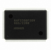
Manufacturer Part Number
DF2398F20V
Description
IC H8S/2300 MCU FLASH 128QFP
Manufacturer
Renesas Electronics America
Series
H8® H8S/2300r
Specifications of DF2398F20V
Core Processor
H8S/2000
Core Size
16-Bit
Speed
20MHz
Connectivity
SCI, SmartCard
Peripherals
DMA, POR, PWM, WDT
Number Of I /o
87
Program Memory Size
256KB (256K x 8)
Program Memory Type
FLASH
Ram Size
8K x 8
Voltage - Supply (vcc/vdd)
4.5 V ~ 5.5 V
Data Converters
A/D 8x10b; D/A 2x8b
Oscillator Type
Internal
Operating Temperature
-20°C ~ 75°C
Package / Case
128-QFP
For Use With
YR0K42378FC000BA - KIT EVAL FOR H8S/2378
Lead Free Status / RoHS Status
Lead free / RoHS Compliant
Eeprom Size
-
Available stocks
Company
Part Number
Manufacturer
Quantity
Price
Company:

Part Number:
DF2398F20V
Manufacturer:
Renesas Electronics America
Quantity:
135
Company:
Part Number:
DF2398F20V
Manufacturer:
Renesas Electronics America
Quantity:
10 000


Bits 11 and 9—Data Transfer Acknowledge (DTA): These bits enable or disable clearing, when DMA transfer is
performed, of the internal interrupt source selected by the data transfer factor setting.
When DTE = 1 and DTA = 1, the internal interrupt source selected by the data transfer factor setting is cleared
automatically by DMA transfer. When DTE = 1 and DTA = 1, the internal interrupt source selected by the data transfer
factor setting does not issue an interrupt request to the CPU or DTC.
When the DTE = 1 and the DTA = 0, the internal interrupt source selected by the data transfer factor setting is not cleared
when a transfer is performed, and can issue an interrupt request to the CPU or DTC in parallel. In this case, the interrupt
source should be cleared by the CPU or DTC transfer.
When the DTE = 0, the internal interrupt source selected by the data transfer factor setting issues an interrupt request to
the CPU or DTC regardless of the DTA bit setting.
The state of the DTME bit does not affect the above operations.
Bit 11—Data Transfer Acknowledge 1 (DTA1): Enables or disables clearing, when DMA transfer is performed, of the
internal interrupt source selected by the channel 1 data transfer factor setting.
Bit 9—Data Transfer Acknowledge 0 (DTA0): Enables or disables clearing, when DMA transfer is performed, of the
internal interrupt source selected by the channel 0 data transfer factor setting.
Bits 10 and 8—Reserved: Can be read or written to. Write 0 to these bits.
Bits 7 and 5—Data Transfer Master Enable (DTME): Together with the DTE bit, these bits control enabling or
disabling of data transfer on the relevant channel. When both the DTME bit and the DTE bit are set to 1, transfer is
enabled for the channel.
If the relevant channel is in the middle of a burst mode transfer when an NMI interrupt is generated, the DTME bit is
cleared, the transfer is interrupted, and bus mastership passes to the CPU. When the DTME bit is subsequently set to 1
again, the interrupted transfer is resumed. In block transfer mode, however, the DTME bit is not cleared by an NMI
interrupt, and transfer is not interrupted.
The conditions for the DTME bit being cleared to 0 are as follows:
The condition for DTME being set to 1 is as follows:
When initialization is performed
When NMI is input in burst mode
When 0 is written to the DTME bit
When 1 is written to DTME after DTME is read as 0
Bit 11
DTA1
0
1
Bit 9
DTA0
0
1
Description
Clearing of selected internal interrupt source at time of DMA transfer is disabled
Clearing of selected internal interrupt source at time of DMA transfer is enabled
Description
Clearing of selected internal interrupt source at time of DMA transfer is disabled
Clearing of selected internal interrupt source at time of DMA transfer is enabled
Rev.6.00 Oct.28.2004 page 187 of 1016
(Initial value)
(Initial value)
REJ09B0138-0600H
Related parts for DF2398F20V
Image
Part Number
Description
Manufacturer
Datasheet
Request
R

Part Number:
Description:
CONN PLUG 12POS DUAL 0.5MM SMD
Manufacturer:
Hirose Electric Co Ltd
Datasheet:
Part Number:
Description:
CONN PLUG 18POS DUAL 0.5MM SMD
Manufacturer:
Hirose Electric Co Ltd
Datasheet:
Part Number:
Description:
CONN PLUG 14POS DUAL 0.5MM SMD
Manufacturer:
Hirose Electric Co Ltd
Datasheet:
Part Number:
Description:
CONN RECEPT 20POS DUAL 0.5MM SMD
Manufacturer:
Hirose Electric Co Ltd
Datasheet:
Part Number:
Description:
CONN PLUG 16POS DUAL 0.5MM SMD
Manufacturer:
Hirose Electric Co Ltd
Datasheet:
Part Number:
Description:
CONN RECEPT 16POS DUAL 0.5MM SMD
Manufacturer:
Hirose Electric Co Ltd
Datasheet:
Part Number:
Description:
CONN PLUG 20POS DUAL 0.5MM SMD
Manufacturer:
Hirose Electric Co Ltd
Datasheet:
Part Number:
Description:
CONN PLUG 30POS DUAL 0.5MM SMD
Manufacturer:
Hirose Electric Co Ltd
Datasheet:
Part Number:
Description:
CONN RECEPT 30POS DUAL 0.5MM SMD
Manufacturer:
Hirose Electric Co Ltd
Datasheet:
Part Number:
Description:
CONN PLUG 40POS DUAL 0.5MM SMD
Manufacturer:
Hirose Electric Co Ltd
Datasheet:

Part Number:
Description:
KIT STARTER FOR M16C/29
Manufacturer:
Renesas Electronics America
Datasheet:

Part Number:
Description:
KIT STARTER FOR R8C/2D
Manufacturer:
Renesas Electronics America
Datasheet:

Part Number:
Description:
R0K33062P STARTER KIT
Manufacturer:
Renesas Electronics America
Datasheet:

Part Number:
Description:
KIT STARTER FOR R8C/23 E8A
Manufacturer:
Renesas Electronics America
Datasheet:

Part Number:
Description:
KIT STARTER FOR R8C/25
Manufacturer:
Renesas Electronics America
Datasheet: