D6417760BP200ADV Renesas Electronics America, D6417760BP200ADV Datasheet - Page 247
D6417760BP200ADV
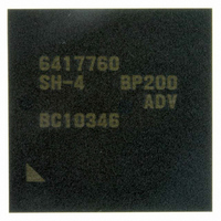
Manufacturer Part Number
D6417760BP200ADV
Description
IC SUPER H MPU ROMLESS 256BGA
Manufacturer
Renesas Electronics America
Series
SuperH® SH7750r
Datasheet
1.D6417760BP200ADV.pdf
(1418 pages)
Specifications of D6417760BP200ADV
Core Processor
SH-4
Core Size
32-Bit
Speed
200MHz
Connectivity
Audio Codec, CAN, EBI/EMI, FIFO, I²C, MFI, MMC, SCI, Serial Sound, SIM, SPI, USB
Peripherals
DMA, LCD, POR, WDT
Number Of I /o
69
Program Memory Type
ROMless
Ram Size
48K x 8
Voltage - Supply (vcc/vdd)
1.4 V ~ 1.6 V
Data Converters
A/D 4x10b
Oscillator Type
Internal
Operating Temperature
-40°C ~ 85°C
Package / Case
256-BGA
Lead Free Status / RoHS Status
Lead free / RoHS Compliant
Eeprom Size
-
Program Memory Size
-
Available stocks
Company
Part Number
Manufacturer
Quantity
Price
Company:

Part Number:
D6417760BP200ADV
Manufacturer:
Renesas Electronics America
Quantity:
10 000


• In double-size cache mode (EMODE = 1 in CCR)
7.3.6
Setting the OIX bit in CCR to 1 enables OC indexing to be performed using bit [25] of the
effective address. This is called OC index mode. In normal mode, with the OIX bit in CCR cleared
to 0, OC indexing is performed using bits [13:5] of the effective address. Using index mode allows
the OC to be handled as two 8-Kbyte areas by means of effective address bit [25], providing
efficient use of the cache. This LSI cannot be used in RAM mode when OC index mode is
selected.
7.3.7
Coherency between cache and external memory should be assured by software. In this LSI, the
following four new instructions are supported for cache operations. Details of these instructions
are given in the Programming Manual.
•
•
•
•
In this mode, the 8 Kbytes comprising entries 256 to 511 of OC way 0 are designated as RAM
area 1 and the 8-Kbytes comprising entries 256 to 511 of OC way 1 are designated as RAM
area 2.
H'7C00 0000 to H'7C00 1FFF (8 Kbytes): Corresponds to RAM area 1
H'7C00 2000 to H'7C00 3FFF (8 Kbytes): Corresponds to RAM area 2
H'7C00 4000 to H'7C00 5FFF (8 Kbytes): Corresponds to RAM area 1
H'7C00 6000 to H'7C00 7FFF (8 Kbytes): Corresponds to RAM area 2
In the same pattern, shadows of the RAM area are created in 16-Kbyte blocks until H'7FFF
FFFF is reached.
Invalidate instruction
Purge instruction
Write-back instruction
Allocate instruction
OC Index Mode
Coherency between Cache and External Memory
:
:
: OCBI @Rn
: OCBP @Rn
: OCBWB @Rn
: MOVCA.L R0,@Rn
Cache invalidation (no write-back)
Cache invalidation (with write-back)
Cache write-back
Cache allocation
:
Rev. 2.00 Feb. 12, 2010 Page 163 of 1330
REJ09B0554-0200
Related parts for D6417760BP200ADV
Image
Part Number
Description
Manufacturer
Datasheet
Request
R

Part Number:
Description:
KIT STARTER FOR M16C/29
Manufacturer:
Renesas Electronics America
Datasheet:

Part Number:
Description:
KIT STARTER FOR R8C/2D
Manufacturer:
Renesas Electronics America
Datasheet:

Part Number:
Description:
R0K33062P STARTER KIT
Manufacturer:
Renesas Electronics America
Datasheet:

Part Number:
Description:
KIT STARTER FOR R8C/23 E8A
Manufacturer:
Renesas Electronics America
Datasheet:

Part Number:
Description:
KIT STARTER FOR R8C/25
Manufacturer:
Renesas Electronics America
Datasheet:

Part Number:
Description:
KIT STARTER H8S2456 SHARPE DSPLY
Manufacturer:
Renesas Electronics America
Datasheet:

Part Number:
Description:
KIT STARTER FOR R8C38C
Manufacturer:
Renesas Electronics America
Datasheet:

Part Number:
Description:
KIT STARTER FOR R8C35C
Manufacturer:
Renesas Electronics America
Datasheet:

Part Number:
Description:
KIT STARTER FOR R8CL3AC+LCD APPS
Manufacturer:
Renesas Electronics America
Datasheet:
Part Number:
Description:
KIT STARTER FOR RX610
Manufacturer:
Renesas Electronics America
Datasheet:

Part Number:
Description:
KIT STARTER FOR R32C/118
Manufacturer:
Renesas Electronics America
Datasheet:

Part Number:
Description:
KIT DEV RSK-R8C/26-29
Manufacturer:
Renesas Electronics America
Datasheet:

Part Number:
Description:
KIT STARTER FOR SH7124
Manufacturer:
Renesas Electronics America
Datasheet:

Part Number:
Description:
KIT STARTER FOR H8SX/1622
Manufacturer:
Renesas Electronics America
Datasheet:

Part Number:
Description:
KIT DEV FOR SH7203
Manufacturer:
Renesas Electronics America
Datasheet: