D6417760BP200ADV Renesas Electronics America, D6417760BP200ADV Datasheet - Page 424
D6417760BP200ADV
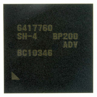
Manufacturer Part Number
D6417760BP200ADV
Description
IC SUPER H MPU ROMLESS 256BGA
Manufacturer
Renesas Electronics America
Series
SuperH® SH7750r
Datasheet
1.D6417760BP200ADV.pdf
(1418 pages)
Specifications of D6417760BP200ADV
Core Processor
SH-4
Core Size
32-Bit
Speed
200MHz
Connectivity
Audio Codec, CAN, EBI/EMI, FIFO, I²C, MFI, MMC, SCI, Serial Sound, SIM, SPI, USB
Peripherals
DMA, LCD, POR, WDT
Number Of I /o
69
Program Memory Type
ROMless
Ram Size
48K x 8
Voltage - Supply (vcc/vdd)
1.4 V ~ 1.6 V
Data Converters
A/D 4x10b
Oscillator Type
Internal
Operating Temperature
-40°C ~ 85°C
Package / Case
256-BGA
Lead Free Status / RoHS Status
Lead free / RoHS Compliant
Eeprom Size
-
Program Memory Size
-
Available stocks
Company
Part Number
Manufacturer
Quantity
Price
Company:

Part Number:
D6417760BP200ADV
Manufacturer:
Renesas Electronics America
Quantity:
10 000


Section 10 Bus State Controller (BSC)
The MRSET bit in MCR selects whether a precharge all banks command or a mode register
setting command is issued. The timing for the precharge all banks command is shown in figure
10.30(1), and the timing for the mode register setting command is shown in figure 10.30(2).
Before setting the mode register, a 200-µs idle time (this is required for the synchronous DRAM
and varies depending on the memory manufacturer) after power is supplied must be guaranteed.
There is no problem in making the precharge all banks setting immediately if the reset signal pulse
width is greater than this idle time.
First, a precharge all banks (PALL) command is issued in the TRp1 cycle by writing to address
H'FF90 0000 + X or H'FF94 0000 + X while the MRSET bit in MCR is cleared to 0. Next, the
number of dummy auto-refresh cycles specified by the manufacturer (usually 8) or more must be
executed. This is achieved automatically while performing various kinds of initialization after the
auto-refresh setting is made, but a more accurate way is to change the RTCOR value only while
these dummy cycles are being executed to set a short interval that generates refresh requests. With
simple read or write access, the address counter in the synchronous DRAM used for auto-
refreshing is not initialized, and so the cycle must always be an auto-refresh cycle. After auto-
refreshing has been executed at least the prescribed number of times, a mode register write
command is issued in the TMw1 cycle by setting MCR.MRSET to 1 and writing to address
H'FF90 0000 + X or H'FF94 0000 + X.
The synchronous DRAM mode register should be configured only once after power-on reset and
before synchronous DRAM access, and the setting should not be changed once it is made.
Rev. 2.00 Feb. 12, 2010 Page 340 of 1330
REJ09B0554-0200
Related parts for D6417760BP200ADV
Image
Part Number
Description
Manufacturer
Datasheet
Request
R

Part Number:
Description:
KIT STARTER FOR M16C/29
Manufacturer:
Renesas Electronics America
Datasheet:

Part Number:
Description:
KIT STARTER FOR R8C/2D
Manufacturer:
Renesas Electronics America
Datasheet:

Part Number:
Description:
R0K33062P STARTER KIT
Manufacturer:
Renesas Electronics America
Datasheet:

Part Number:
Description:
KIT STARTER FOR R8C/23 E8A
Manufacturer:
Renesas Electronics America
Datasheet:

Part Number:
Description:
KIT STARTER FOR R8C/25
Manufacturer:
Renesas Electronics America
Datasheet:

Part Number:
Description:
KIT STARTER H8S2456 SHARPE DSPLY
Manufacturer:
Renesas Electronics America
Datasheet:

Part Number:
Description:
KIT STARTER FOR R8C38C
Manufacturer:
Renesas Electronics America
Datasheet:

Part Number:
Description:
KIT STARTER FOR R8C35C
Manufacturer:
Renesas Electronics America
Datasheet:

Part Number:
Description:
KIT STARTER FOR R8CL3AC+LCD APPS
Manufacturer:
Renesas Electronics America
Datasheet:
Part Number:
Description:
KIT STARTER FOR RX610
Manufacturer:
Renesas Electronics America
Datasheet:

Part Number:
Description:
KIT STARTER FOR R32C/118
Manufacturer:
Renesas Electronics America
Datasheet:

Part Number:
Description:
KIT DEV RSK-R8C/26-29
Manufacturer:
Renesas Electronics America
Datasheet:

Part Number:
Description:
KIT STARTER FOR SH7124
Manufacturer:
Renesas Electronics America
Datasheet:

Part Number:
Description:
KIT STARTER FOR H8SX/1622
Manufacturer:
Renesas Electronics America
Datasheet:

Part Number:
Description:
KIT DEV FOR SH7203
Manufacturer:
Renesas Electronics America
Datasheet: